CNSE Innovation Lab

CNSE Innovation Lab Home

CNSE Innovation Lab University at Albany State University of New York

The CNSE Innovation Lab is a collection of academic cleanrooms and labs that provide partners with strategic support through technology acceleration, proof of concept, pilot prototyping, and test-bed integration support for “next generation” nanotechnology research activities. Projects processed in these labs tend to focus on traditional and emerging applications in the areas of nanoelectronics, microsystems, nanobioscience, and clean energy.

The CNSE Innovation Lab contains a full complement of leading-edge tools to convert ideas into reality with process capabilities that include: thin film deposition, wet etch, deep reactive ion etch, dry etch, wafer bonding, polymer processing, wafer patterning, handling of multiple wafer sizes up to 200mm and materials, rapid thermal anneal, and ion implantation. Projects processed within these labs not only have access to CNSE faculty subject matter experts, but also the co-located semiconductor supply chain for rapid manufacturing scale up.

See our current tool catalog. If there is something you wish to use, but do not see, please ask.

For more information on our engagement models or to schedule time to tour the facility please contact the CNSE Innovation Lab Manager Bryant Colwill at [email protected].


Examples of some of these devices and subsystems include:

  • MEMs
  • BioMEMS
  • RF MEMS
  • Microfluidics
  • Micro-optics
  • NanoBio
  • Nano and micro technology
  • 3-D wafer processing


Device and Micro System Simulation and Modeling

Micro Systems and devices are first created by utilizing state-of-the-art simulation and modeling tools which include IntelliSuite and ANSYS.


Mask Layout

After simulation and modeling, the final designs of the devices are laid out using L-Edit to produce photo masks. L-Edit is a VLSI design tool; it is flexible enough to do micromachining design, printed circuit board layout and other CAD work.

CNSE's professors and professional staff welcome the challenge of developing unique devices and processes with our partners.


Processing Capabilities

  • 100 to 200 mm Substrates
    • - Silicon, Glass, Ceramic, Polymer
  • Standard and Custom Processes Supported
  • Thin Film Deposition
  • Patterning
  • Etching
  • Bonding
  • CMP
  • Complete Metrology Suite
Current Tool Catalog

Recently Installed Tools

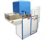
2023 OXFORD FLEX AL ALD

The Flex Al system can deposit highly conformal coatings by both thermal and plasma enhanced deposition modes. The heated chuck has a maximum operating temperature of 500˚C and system is equipped with six precursor ampules.

SAMPLE SIZE: Pieces through 8" Wafers

TEMPERATURE RANGE: RT-500C

PROCESS GASES: NH3, H2, C4F8, O2, Ar, N2

2023 OXFORD FLEX AL ALD
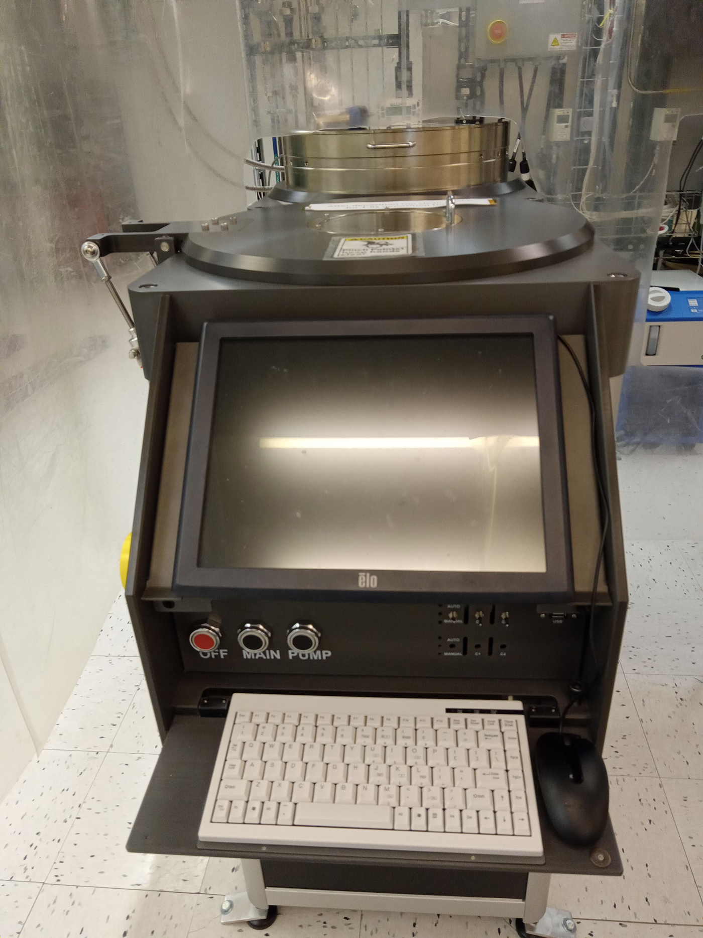
TRION PECVD

This plasma system deposits silicon dioxide, silicon nitride and a-Si films. Use of the triode generator (600W) can allow for custom film property tailoring for parameters such as stress and stoichiometry. 

SAMPLE SIZE: Pieces through 8'’ Wafers

TEMPERATURE RANGE: RT- 400˚C

PROCESS GASES: NH3, N2O, O2,CF4, N2, SiH4, He

TRION PECVD
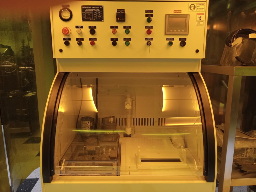
REYNOLDS ELECTROCHEMICAL DEPOSITION

This electroplating station provides a heated recirculated bath for nickel plating chemistries and an integrated overflow rinse tank. 

SAMPLE SIZE: Pieces through 8'’ Wafers

TEMPERATURE RANGE: RT- 400˚C

PROCESS GASES: NH3, N2O, O2,CF4, N2, SiH4, He

REYNOLDS ELECTROCHEMICAL DEPOSITION
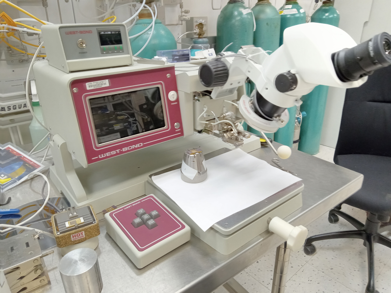
WEST BOND 7KFH WIRE BONDER

Manual wire bonder can be used in either wedge and ball bonding modes. System is currently equipped with 25um aluminum wire. 

SAMPLE SIZE: Pieces and packages. 

TEMPERATURE RANGE: Up to 150˚C

WEST BOND 7KFH WIRE BONDER
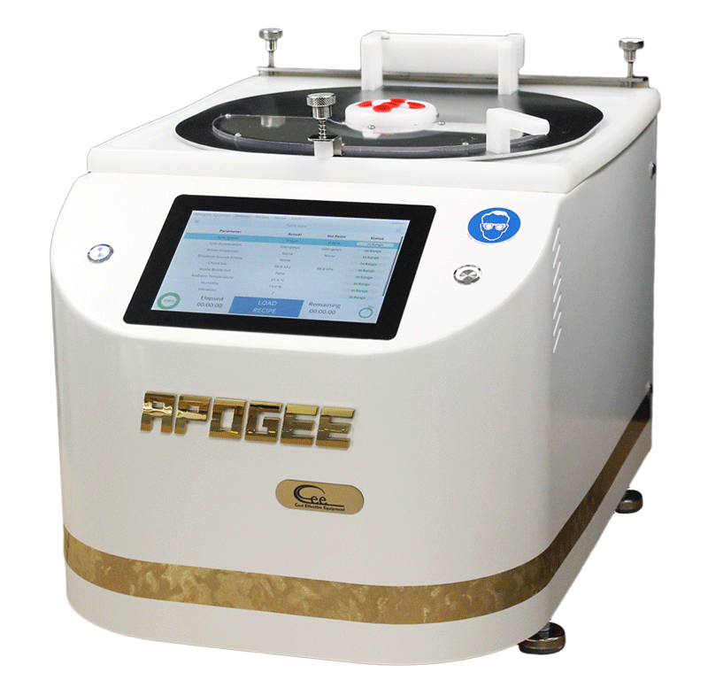
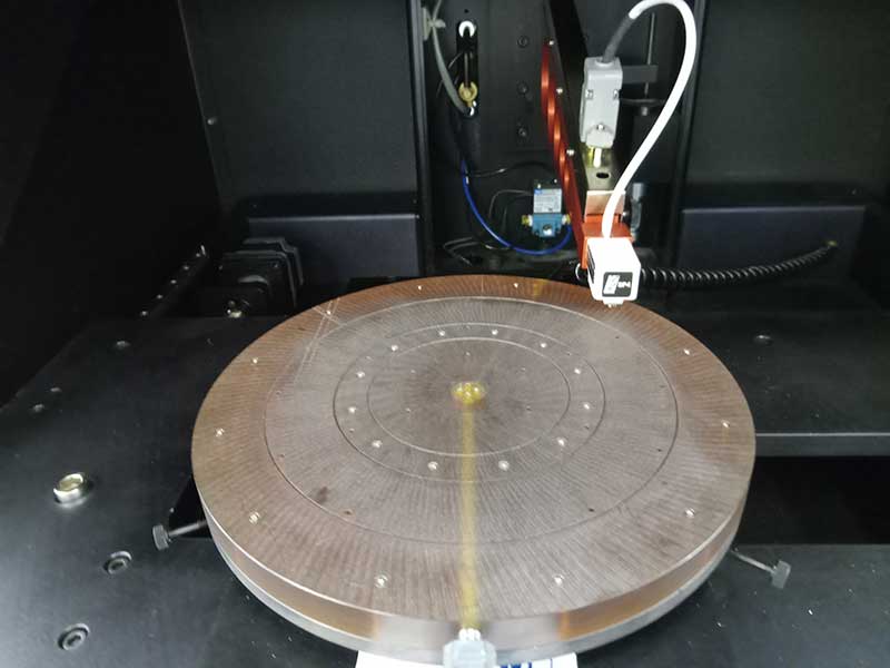
APOGEE SPIN COATER/BAKE SYSTEM

The spinner can be used for applying resist and other spin-on films on up to 200 mm wafers. The bake plate can be configured for proximity and contact baking at various temperatures ranging from room temperature to 300˚C.

SAMPLE SIZE: Pieces through 8'’ Wafers

TEMPERATURE RANGE: RT-300C

PROCESS GASES: Purge N2

APOGEE SPIN COATER/BAKE SYSTEM
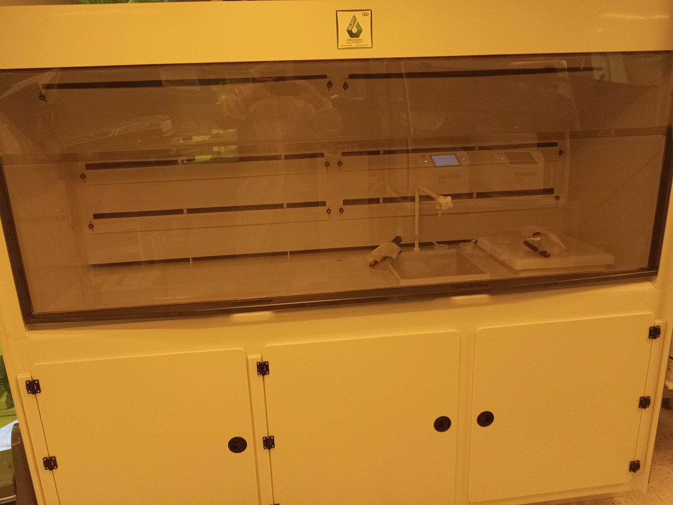
BURT WET BENCH

Dedicated for aqueous chemistries used for wet etching and surface preparatory cleans. Commonly
used for RCA, Piranha, HF etching, etc.

SAMPLE SIZE: Pieces through 8'’ Wafers 

RESTRICTED MATERIALS: Contact staff for heavy metals including Au and Cr.

BURT WET BENCH

Pre Existing Tools

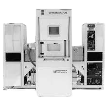
PLASMA-THERM VERSALOCK 700

PLASMA-THERM VERSALOCK 700 The Plasma-Therm Versalock 700 is a ICP dry etch tool with two chambers. One etches traditional silicon based semiconductor films (nitrides/oxides) while the other chamber supports etching high aspect silicon structures using the Bosch process (DRIE).

SAMPLE SIZE: Pieces through 8'’ Wafers

TEMPERATURE RANGE: Chuck: 25˚C

PROCESS GASES: C4F8, CHF3, CF4, SF6, Ar, O2, N2

PLASMA-THERM VERSALOCK 700
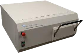
SOLARIS 150 RAPID THERMAL PROCESSING

Rapid thermal processing system with the temperature range up to 1100˚C with soak times on the scale of seconds to minutes. Annealing is done in an N2 ambient atmosphere.

SAMPLE SIZE: Pieces through 4" Wafers

TEMPERATURE RANGE: 300˚C - 1000˚C

SOLARIS 150 RAPID THERMAL PROCESSING
OAI MODEL 800 CONTACT ALIGNER

OAI Model 800 contact aligner is a broadband lithography exposure system that use a stable mercury light source. It has both front and backside cameras for alignment and can expose in proximity, vacuum contact or hard contact. Minimum resolution is approximately 1um and level to level overlay is typically several microns. 

SAMPLE SIZE: Pieces through 8'’ Wafers

OAI MODEL 800 CONTACT ALIGNER
TRION MINILOCK III ICP-RIE ETCH TOOL

The Trion Minilock is an ICP-RIE plasma etcher that utilizes both chlorinated and fluorinated chemistries. The dual RF generators allow for independent control of both the plasma density and acceleration bias. 

SAMPLE SIZE: Pieces through 8'’ Wafers

TEMPERATURE RANGE: Chuck: 0-20˚C

PROCESS GASES: Cl2, BCl3, CHF3, CF4, O2, SF6, Ar, He

TRION MINILOCK III ICP-RIE ETCH TOOL
SHARON E-BEAM EVAPORATOR

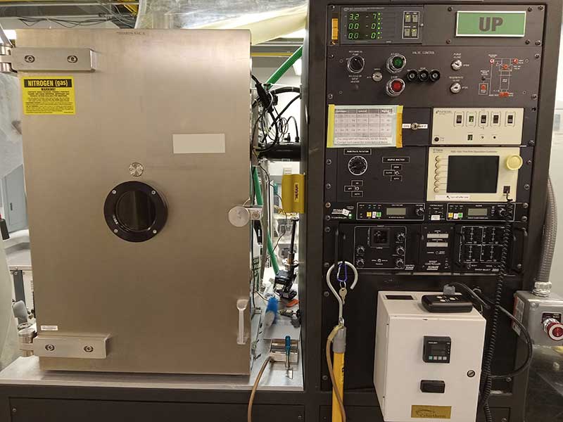
Electron beam evaporator for depositing thin, high purity metal films. The system is cryo pumped and has a 6 pocket hearth. Film thickness is monitored during deposition via QCM.

SAMPLE SIZE: Pieces through 8'’ Wafers


SHARON E-BEAM EVAPORATOR
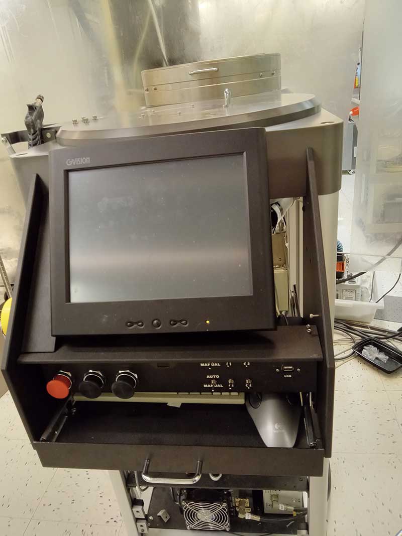
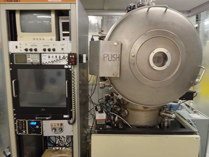
VARIAN 980 E-BEAM EVAPORATOR

Electron beam evaporator for depositing thin, high purity, films. Has a large chamber for large numbers of wafers. Four packet hearth allows for successive depositions of stacked material without the need for breaking vacuum. Film thickness is monitored during deposition via QCM. 

SAMPLE SIZE: Pieces through 12" Wafers

VARIAN 980 E-BEAM EVAPORATOR
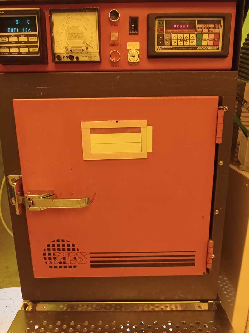
YES PRIMING OVEN

The oven is used for HDMS priming substrates prior to lithography resist applications. 

SAMPLE SIZE: Pieces through 8'’ Wafers 

TEMPERATURE RANGE: 50C-200C 

PROCESS GASES: HMDS Vapor

YES PRIMING OVEN
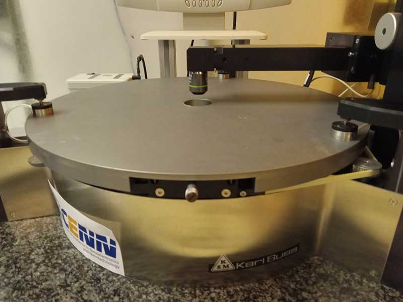
ZEISS DSM DOUBLE SIDE MEASURING SYSTEM

The system has two cameras and measures the accuracy of front-back side alignment on up to 300 mm wafers 

SAMPLE SIZE: 3" through 12" Wafers

ZEISS DSM DOUBLE SIDE MEASURING SYSTEM
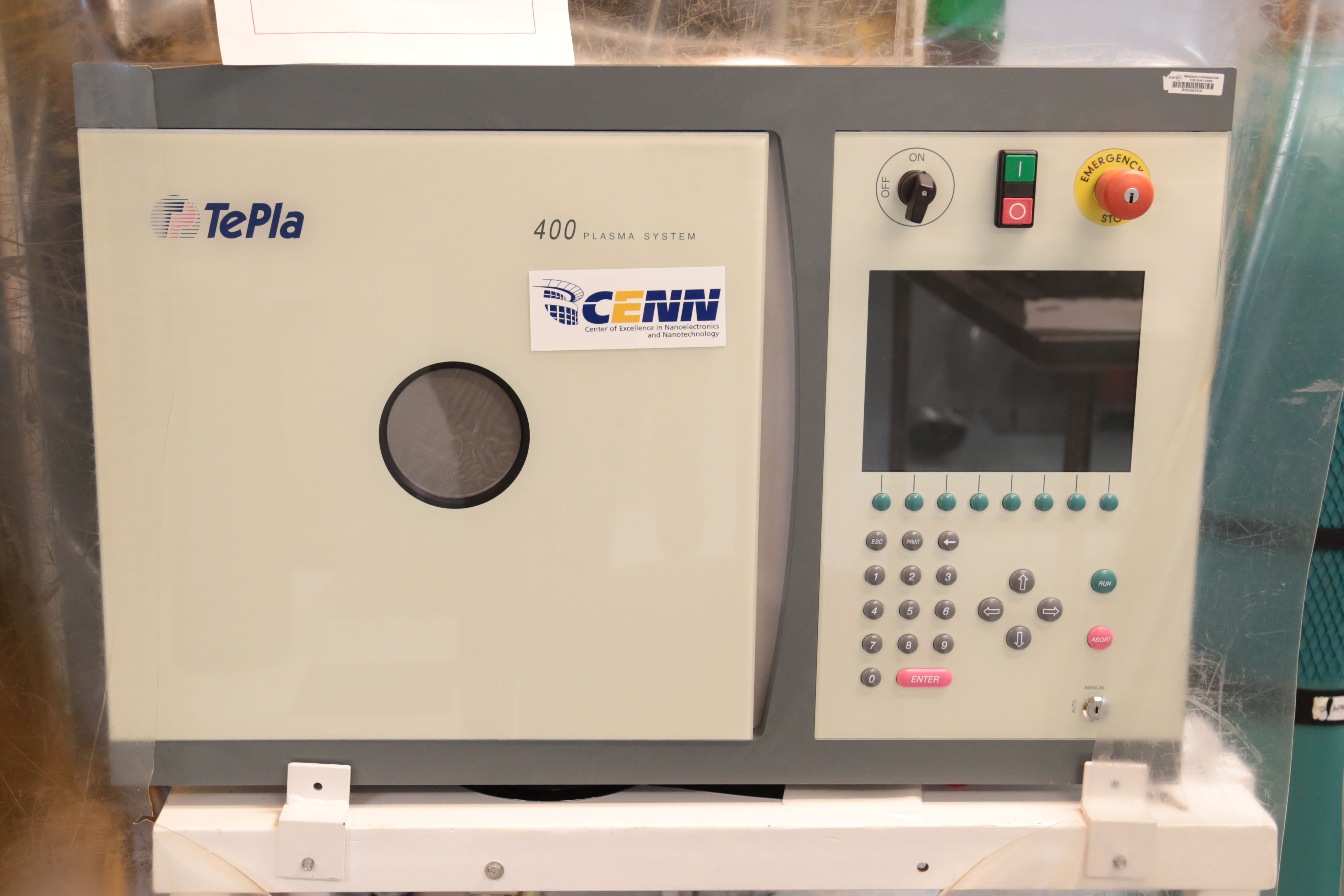
TEPLA 400 PLASMA SYSTEM

TePla 400 Plasma System cleans, modifies surfaces with an oxygen and/or argon plasma. 

SAMPLE SIZE: Pieces through 8'’ Wafers 

PROCESS GASES: O2, Ar

TEPLA 400 PLASMA SYSTEM
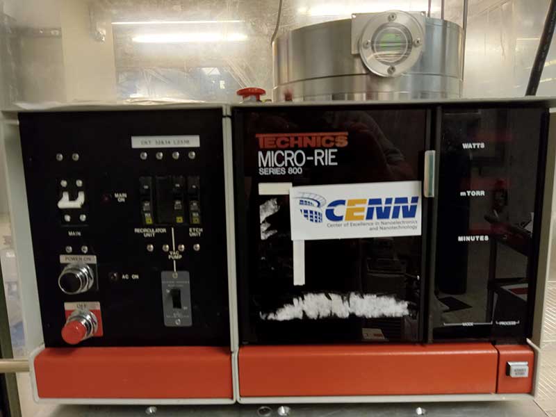
TECHNICS MICRO RIE SERIES 800

Classical parallel plate RIE system can used to etch silicon based films with fluorinated chemistries. 

SAMPLE SIZE: Pieces through 3" Wafers 

PROCESS GASES: CF4, SF6, CHF3, O2

TECHNICS MICRO RIE SERIES 800
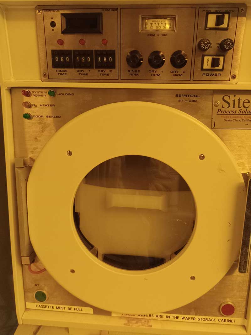
SPIN RINSE DRYER

The systems rinses samples with DI water and then flows heated nitrogen to thoroughly dry. Only whole semi-standard 6" and 8" wafers can be accommodated. 

SAMPLE SIZE: Pieces through 6'’ and 8'’ Wafers 

PROCESS GASES: Purge N2

RESTRICTED MATERIALS: Silicon Wafers only.

SPIN RINSE DRYER
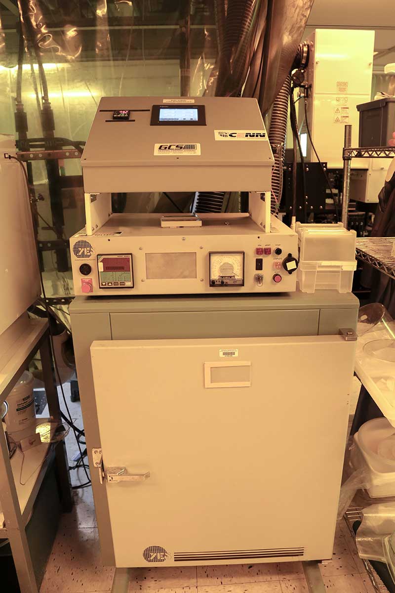
YES CURING OVEN

Curing oven up to 450˚C in nitrogen. Can be used for polymeric curing and reflow.

SAMPLE SIZE: Pieces through 8'’ Wafers

TEMPERATURE RANGE: 

PROCESS GASES: N2

YES CURING OVEN
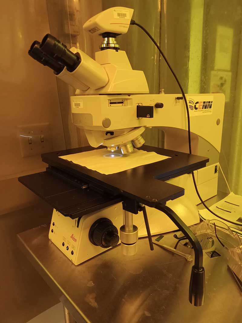
LEICA DM8000 OPTICAL MICROSCOPE

The optical microscope is equipped with magnification lens of 5x, 10x, 20x, 50x and 100x. The system uses an LED based illuminator and is connected to a digital camera with imaging software.  

SAMPLE SIZE: Pieces through 8'’ Wafers

LEICA DM8000 OPTICAL MICROSCOPE
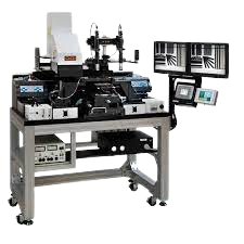
SIGNATONE QUADPROS-A8

Semiautomatic probe station for measuring film thickness or resistivity. Can be programmed to map across sample uniformity. 

SAMPLE SIZE: Pieces through 8'’ Wafers

SIGNATONE QUADPROS-A8
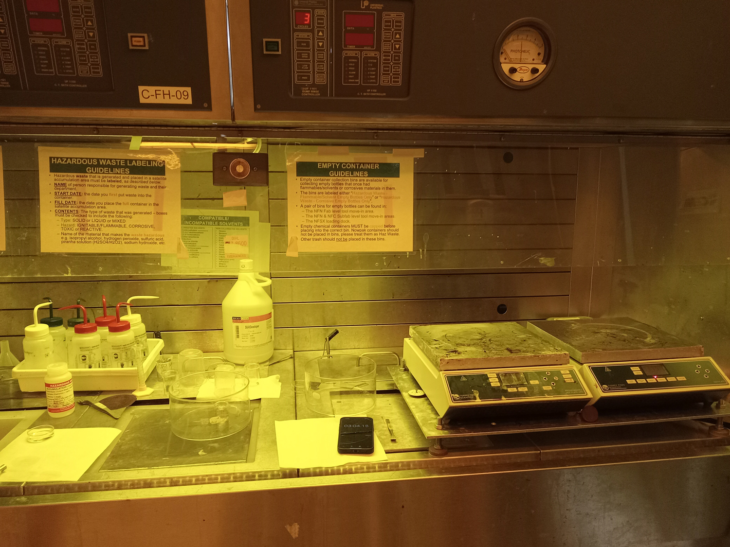
DEXON 855PS-5 SOLVENT BENCH

General purpose solvent bench for sample solvent cleaning and SU-8 resist development. 

SAMPLE SIZE: Pieces through 8'’ Wafers

DEXON 855PS-5 SOLVENT BENCH
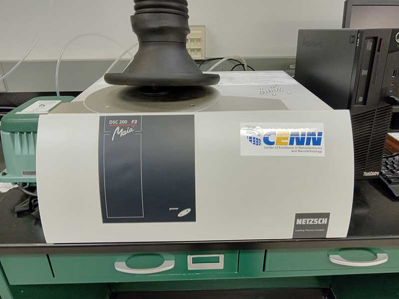
DIFFERENTIAL SCANNING CALORIMETER

The calorimeter can be used to extract important material characteristics such as melting point, glass transition temperature, decomposition point and polymorphism. Samples are loaded in a small crucible and place in an isothermically controlled furnace.

SAMPLE SIZE: Milligrams 

TEMPERATURE RANGE: RT-600˚C

RESTRICTED MATERIALS: Toxics

DIFFERENTIAL SCANNING CALORIMETER
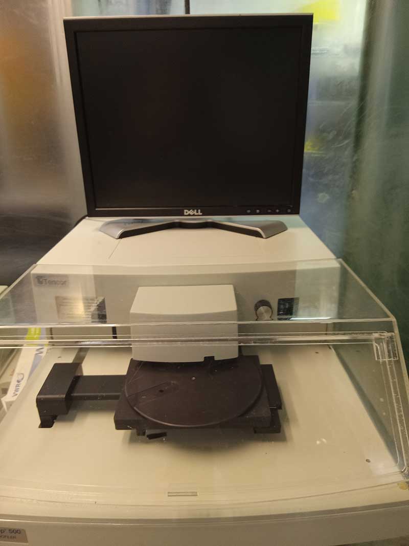
KLA TENCOR ALPHA-STEP 500 PROFILOMETER

The KLA Tencor Alpha-Step 500 Profilometer can measure step height for deposited or etched films. The maximum scan length is 5mm and maximum vertical step is limited to under 300um. At the highest resolution settings, a step height as small as 50nm can be quantified. 

SAMPLE SIZE: Pieces through 6'’ Wafers

KLA TENCOR ALPHA-STEP 500 PROFILOMETER
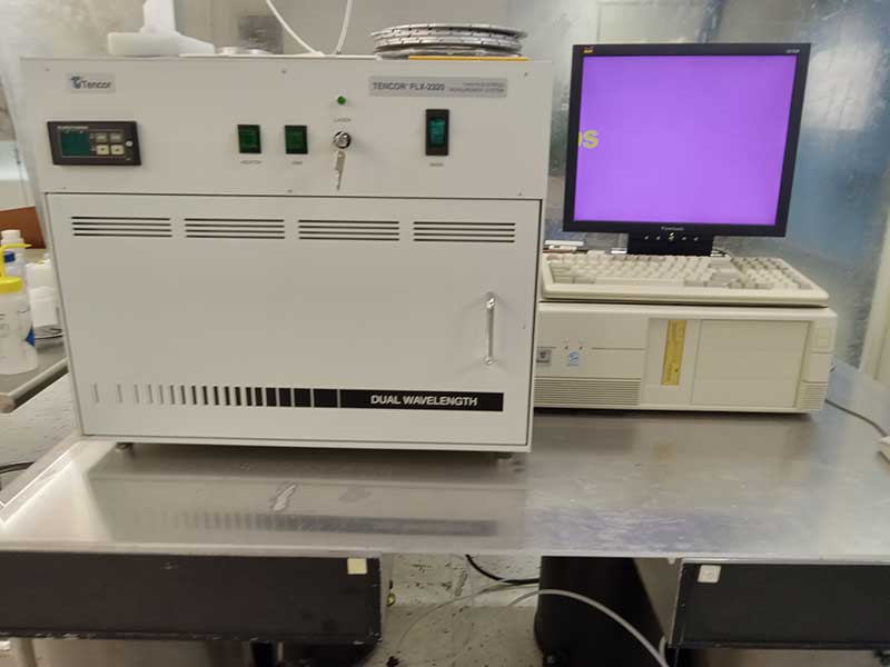
KLA TENCOR FLX-2320 FILM STRESS PROBE

Non-contact technique to measure wafer curvature. Applied pre/post deposition the measurements are used to determine deposited film stress. Stage temperature can also be controlled to extract material thermal coefficient of expansion.

SAMPLE SIZE: 3" through 8" Wafers 

TEMPERATURE RANGE: RT - 300˚C

KLA TENCOR FLX-2320 FILM STRESS PROBE
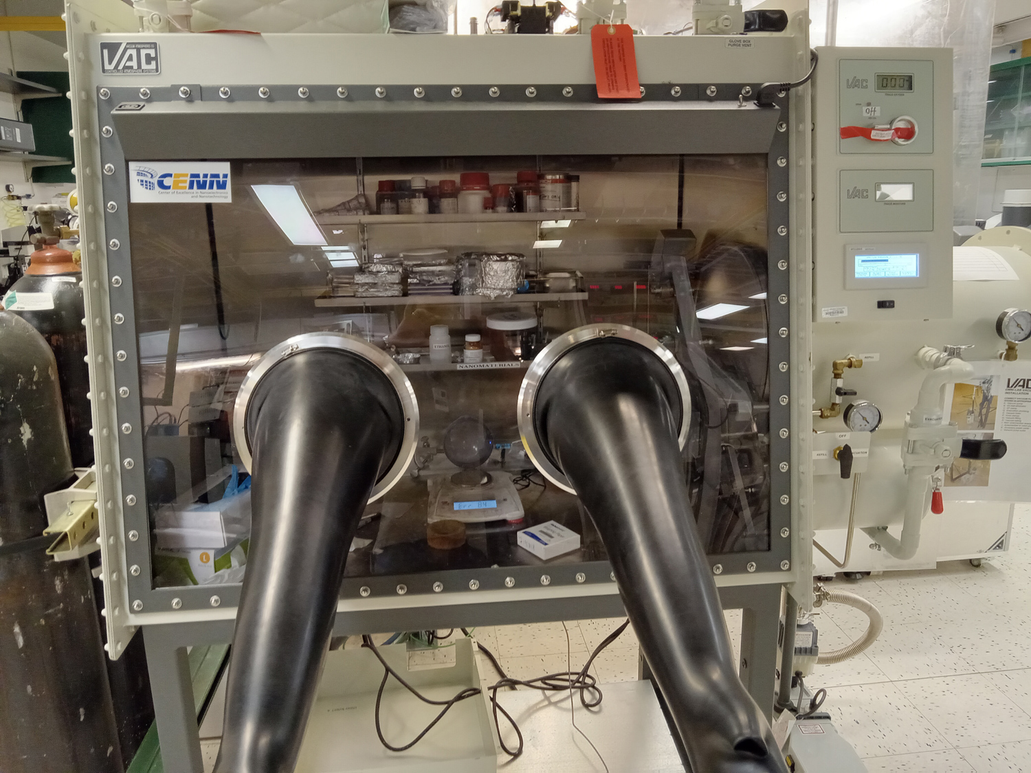
VACUUM ATMOSPHERES OMNILAB GLOVE BOX

An positive pressure N2 workspace that allows for handling and packaging of O2 and H2O sensitive materials. The large ante-chamber allows for the efficient passthrough materials and ancillary equipment that may be required for use with sensitive materials. 

SAMPLE SIZE: Pieces through 8'’ Wafers 

PROCESS GASES: N2 Purge

VACUUM ATMOSPHERES OMNILAB GLOVE BOX


If there is something you wish to use, but do not see, please ask.