


UAlbany Launches New Programs in Semiconductor Engineering
ALBANY, N.Y. (Aug. 21, 2024) —The University at Albany’s College of Nanotechnology, Science, and Engineering has launched three new graduate certificate programs in semiconductor engineering.
The programs are designed to meet the demand for a skilled workforce in the U.S. and global semiconductor industry, a market that is expected to reach $1 trillion annually by the end of the decade.
The new programs are a critical component of New York’s landmark investments in semiconductor R&D, much of it at the Fuller Road Albany NanoTech Complex owned and operated by NY CREATES, and will help supply the skilled workforce needed to realize the ambitious economic and national security goals of the $53 billion federal CHIPS & Science Act.
A recent analysis by McKinsey & Co. forecast as many as 10,000 new semiconductor-related jobs in New York alone as the Capital Region makes its case as a leading contender to be part of the National Semiconductor Technology Center, a major R&D effort funded by the CHIPS Act.
Innovative Academics
The programs, housed within UAlbany’s Department of Nanoscale Science and Engineering, include graduate certificates in Semiconductor Manufacturing, Semiconductor Patterning and Processing and Semiconductor Metrology. They are now active and recruiting students for the fall 2024 semester.
The launch of the programs follows several important strategic investments in UAlbany’s burgeoning College of Nanotechnology, Science, and Engineering, as well as other significant investments across New York State, including the $10 billion partnership announced by Gov. Kathy Hochul to build the nation’s first High NA Extreme Ultraviolet Lithography Center at the NY CREATES Albany NanoTech Complex, the $40 million Northeast Regional Defense Technology Hub (NORDTECH), as well as the Center for Emerging Artificial Intelligence Systems (a $20 million collaboration between UAlbany and IBM).
In addition, UAlbany is continuing to expand its academic and research footprint in artificial intelligence through the AI Plus initiative, hallmarked by first-in-the-nation supercomputing collaborations with NVIDIA to adopt the NVIDIA DGX Cloud and with IBM to install the first prototype IBM Artificial Intelligence Unit (IBM AIU) at a university to advance generative AI research.
“The University at Albany is proud to be offering three new graduate certificates in semiconductor engineering that will help provide the semiconductor industry with the skilled workforce it needs to continue to grow in the Capital Region and across New York,” said University at Albany President Havidán Rodríguez. “Strong partnerships between industry and higher education – like UAlbany’s partnerships with NY CREATES , IBM, and others – are critical to New York’s continued leadership in the semiconductor industry. As one of the nation’s most diverse public research institutions, we are working to ensure the growth of this industry benefits all New Yorkers.”
“For more than 20 years, UAlbany has been developing academic programs that help the semiconductor industry meet its needs,” said UAlbany Provost and Senior Vice President Carol Kim. “These new programs are just the latest example. We’re very pleased to be providing a bridge between potential students and this exciting high-tech sector.”
Responding to Workforce Needs
“The connection between the academic programs and research of CNSE and the semiconductor industry is unsurpassed in this country. By sharing space with the leading chip design and manufacturing companies at Albany NanoTech, the faculty of our Department of Nanoscale Science & Engineering are in daily conversations about the direction and needs of the industry. These new graduate certificates have been developed in response to those needs, and they are just the first step in our new academic efforts. Additional graduate certificates in business aspects related to the industry as well as other focused technical topics are under development, as well as a growing portfolio of skill-focused microcredentials,” said CNSE Dean Michele J. Grimm.
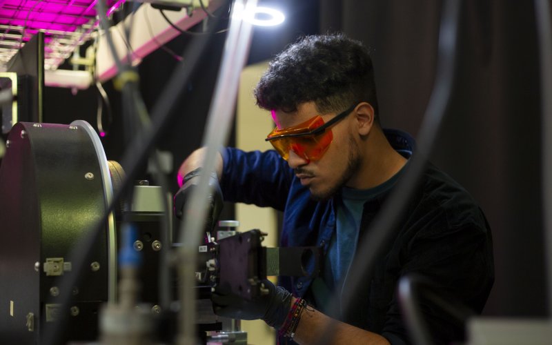
Students enrolled in the programs will be provided examples drawn from the 300 mm wafer fabrication line at Albany NanoTech. The programs are designed for professionals working in the semiconductor industry who want to learn new skills, increase the depth of their knowledge and advance their careers. The graduate certificates can be completed entirely online, although not all courses are offered remotely. An undergraduate degree in a related area of engineering, physics, chemistry, or similar is required for students seeking to enroll in the new graduate certificate programs.
Manufacturing
The Graduate Certificate in Semiconductor Manufacturing provides a comprehensive overview of the semiconductor and microelectronics manufacturing process, beginning with the science of materials used in microelectronics manufacturing, microelectronic device architecture and operation, wafer processing and patterning technologies, quality control and device performance and reliability.
Following completion of the program, students will understand the design and operating principles of semiconductor devices, the general principles of the processing and lithographic technologies used in the fabrication of microelectronic devices and the considerations for integrating the fabrication steps into a process flow.
Patterning and Processing
The Graduate Certificate in Semiconductor Patterning and Processing provides in-depth understanding of the lithographic, deposition and etch processes and technologies used in the fabrication of microelectronics on wafers. Particular attention is given to determining optimal operating conditions for meeting target design specifications.
Students completing the program will have an in-depth understanding of the principal thin-film processing technologies used in state-of-the-art microelectronics fabrication, including deposition, etch and extreme ultraviolet lithography.
Metrology
The Graduate Certificate in Semiconductor Metrology provides both a practical and theoretical foundation for professionals who need to understand operational fundamentals and physical principles that underly semiconductor metrology for high volume manufacturing. The program focuses on the metrology methods used for measuring statistical process variations that affect yield, as well as design of sampling strategies and data interpretation. Students will learn broad principles of metrology and will gain an in-depth understanding of techniques of their choosing.
Students completing this program will have an in-depth understanding of the principles of semiconductor metrology and the classes of measurements made during high volume manufacturing of semiconductors. Students will also develop a working knowledge of the major semiconductor metrology methods used and the challenges presented by sub-nanometer precision requirements.