Wide Band Gap Optronix Lab

Wide Band Gap Optronix Lab

Wide Band Gap Optronix Lab tool


Our program is primarily focused on the development of wide bandgap III-Nitride materials and devices. III-Nitride materials are among the most technologically important material systems with a variety of applications ranging from single photon detection (e.g. APDs and Cs-free photocathodes) to quantum computing and astronomy applications, high brightness LEDs for solid state lighting, lasers for high density optical storage systems, UV and green emitters for water purification and biological agent detection and communication, to high power RF transistors for cell phone and satellite communication, switching and amplification, and for application as harsh environment sensors, to name a few.

The field of III-Nitride semiconductors (AlxInyGa1-x-yN, 0<x, y<1), is focused on developing a new class of semiconductors that have certain unique properties as compared to conventional semiconductors such as Si and GaAs. The enabling properties are the wide and direct band gap, and the ability for bandgap engineering (adjustable from 0.9 eV for InN to 3.4eV for GaN to 6.2 eV for AlN), high breakdown voltage, and high saturation velocity. Metalorganic chemical vapor deposition (MOCVD) is used for the development of the AlInGaN-based structures. Variety of characterization techniques are used for the study of optical, structural, morphological and electrical properties of the layers and device structures.

Funding Sources

Wide Band Gap Optronix Lab
Dr. Fatemeh (Shadi) Shahedipour-Sandvik

257 Fuller Road
Albany, NY 12203
United States

Phone
Phone 2
Fax
518-437-8687

Research

If you're interested in our work or want to work with us, email [email protected].

Current Projects
Novel dopant activation techniques for high voltage GaN power devices

Selective doping is required in a number of device designs including current aperture vertical electron transistors (CAVET), vertical junction FETs, and junction barrier Schottky (JBS) diodes to form junction termination extension structures. This enables high voltage, high power, and high frequency GaN power devices for applications in radar, vehicle drivetrain, power grid, and other power electronics. Implementing selective-area ion implantation to obtain p-type III-nitrides remains challenging due to the temperature required to repair defects and locate the p-type dopant, Mg, in substitutional sites. Achieving selective-area p-doping through Mg implantation requires an activation anneal at temperatures beyond the region of thermodynamic stability in GaN. This requires nonequilibrium annealing conditions to activate the material without inducing degradation.

We are developing a process to achieve acceptor activation by rapid, high temperature pulsing using a novel application of a gyrotron microwave beam. At temperatures of >1300 °C for duration of 1 min, p-type activation by gyrotron of Mg-implanted GaN has been observed by optical and electrical characterization. Photoluminescence measurements show 1.6X higher emission intensity in the Mg related UVL over VN related GL2 band, representing a regime that anneal-activated Mg acceptor concentration is beyond compensating donor defects.  Measurement of device shows characteristics of p-n diode with a turn-on voltage of 3.0 V. Gyrotron annealing also proves effective at recovering implant-induced lattice damage, increasing in effectiveness with annealing temperatures from 1150 °C to 1350 °C, as measured by XRD. These structural, optical, and electrical measurements point to the promise of the gyrotron annealing technique for selective p-doping for its implementation in power devices.

Diagram 1A
Diagram 1B

Figure 1. (left) Schematic diagram of novel gyrotron annealing system used for high temperature annealing above 1300 °C for activation of the Mg-dopant (right) heating diagram showing thermal pulsing to 1350 °C

Figure 2A
Figure 2B

Figure 2. (left) Diode I-V from Mg-implanted GaN annealed by gyrotron at 1350 °C showing p-n diode characteristics and (right) low-temperature (20 K) photoluminescence spectra of gyrotron annealed samples. Sample annealed at 1350 °C shows 1.6X stronger Mg related UVL over VN related GL2 band, representing a regime that anneal-activated Mg acceptor concentration is beyond compensating donor defects.

Enhanced Reliability and Performance of High Electron Mobility Transistors for Power Systems

AlGaN/GaN heterostructures possess a two-dimensional electron gas (2DEG) formed due to the presence of spontaneous and piezoelectric polarization. This two-dimensional channel can be modulated with a gate to form transistors. We have implemented dynamic body-bias technique to improve the performance of AlGaN/GaN HEMTs with the successful integration of a body-diode. In this configuration, p-GaN body-diode-based back-gate control is used to shift the threshold voltage and dynamically modulate the ON/OFF characteristics of a normally-ON AlGaN/GaN HEMT. A fourth back-gate terminal is connected to the p-GaN layer to control the depletion width of the body-diode, which in turn modulates the 2DEG density.

GAN

Figure 1. Variation of charge distribution in depletion and 2DEG channel region with the application of positive, negative, and zero bias to the back-gate terminal.


Enhanced Reliability and Performance of High Electron Mobility_Fig2A
Enhanced Reliability and Performance of High Electron Mobility_Fig2B


Figure 2. (left) Four terminal transfer characteristics at VDS=0.5 showing the shift in the top-gate threshold voltage with the application of different back-gate voltages and (right) variation of the top-gate threshold voltage as a function of back-gate voltage.


In collaboration with Army Research Lab (ARL), we have been working to develop power HEMT devices with improved reliability and performance. We utilize passivation dielectric to reduce current collapse and gate dielectric to reduce gate-leakage current. However, the introduction of a dielectric layer leads to issues associated with the dielectric/(Al)GaN interface trap states, bulk trap states within the dielectric, and surface defect states which can negatively affect performance. We are exploring different dielectric materials including aluminum oxide, silicon dioxide, and silicon nitride deposited using atomic layer deposition. In order to decrease the density of trap states, various pre- and post-deposition treatments, such as annealing in forming gas ambient, are utilized. In order to evaluate the dielectric and dielectric/semiconductor interface, we fabricate metal-insulator-semiconductor (MIS) capacitors and measure the capacitance-voltage (C-V) behavior to determine the amount of charge trapped in the dielectric and at the interface.

Figure 3 GAN

Figure 3. C-V measurement data of Al2O3 MIS capacitors with post-dielectric deposition annealing in forming gas at (a) 350 °C for 1 min, (b) 350 °C for 10 min, (c) 350 °C for 20 min, (d) 600 °C for 1 min, (e) 475 °C for 10 min, (f) 600 °C for 20 min, and (g) as-deposited. The arrows indicate the direction of the DC bias sweep. Insets show zoomed in area of hysteresis to show ΔV from sweep up to sweep down. Reduction in hysteresis, indicating reduced trapped charge density, is observed after annealing at low temperature for extended times, while high temperature annealing results in increased trap density.

Cs-free polarization-engineered III-Nitride photocathode

III-Nitride based photocathodes have been the subject of much research in photoemissive devices for ultraviolet detection in astronomy, planetary or defense applications. In order to achieve high quantum efficiency (QE), negative electron affinity (NEA) is necessary. NEA is conventionally reached via surface cesiation which requires special in-situ fabrication steps, including cleaning and activation in vacuum and sealed-tube packaging, due to Cesium’s high chemical activity. Photocathodes using this technology have been reported to suffer from chemical instability and QE degradation over time.

Recent work has been performed to eliminate Cs-based surface treatments and improve device efficiency by taking advantage of the polarization exhibited by III-Nitrides in order to achieve NEA. Previously, we developed and reported a novel Cs-free GaN photocathode based on Si-delta-doping. While improved performance was observed with the use of Si-delta doping, the high dopant concentration results in increased scattering.

We have proposed and investigated novel Cs-free III-Nitride photocathodes that show permanent NEA without the use of delta-doping and thus show potential for higher QE. By replacing Cs-based surface treatments with polarization engineering to affect surface properties, we allow the device to be air stable. Additionally, polarization engineering is used as an alternative to impurity-based doping in order to allow high free carrier concentrations without a decrease in mobility. Devices have been studied via both simulation and photoemission measurements of devices grown via MOCVD. In support of our work to achieve high-efficiency photocathodes, we are engaged in fundamental studies on enhancement of p-type conductivity and surface engineering in N-polar III-Nitride materials.

Cs-free polarization-engineered_Fig1

Figure 1. Schematic band diagram of III-Nitride photocathode with photon incident on the semiconductor surface.
The photodetector absorbs photons with sufficient energy, creating photoexcited carriers which transport to the
surface aided by an intern electric field, and are emitted into vacuum and counted.


Figure 2 GAN
Figure 3 GAN


Figure 2. (left) Photoemission spectroscopy shows the highest quantum efficiency for photocathode structures grown on a high hillock density film  (Right) Atom probe tomography (APT) reconstructions showing a decrease in Mg-clustering within hillock structures which allows for a greater probability for Mg-atoms to act as acceptors within the film, increasing the quantum efficiency

(Al)GaN-based Betavoltaic Microbatteries

Conventional lithium batteries, although low in cost, expel energy relatively quickly and require replacement. Betavoltaic (BV) batteries show promise as a replacement in low power (nW-µW) applications due to high energy density, relatively low weight and long lifetime. A BV device is analogous to a solar cell, where electron hole pairs (EHPs) are created by incident radiation. The radiation source in a BV device are high energy electrons, or β-particles, emitted from a coupled radioactive isotope. The kinetic energy of these β-particles dissipates throughout a semiconductor material through creation of EHPs by impact ionization and losses due to numerous scattering mechanisms.

Using electron beam induced current (EBIC) we have reported GaN planar n-i-p devices with output powers of 70 nW and 640nW with quantum efficiencies of 1.2% and 4.0% at electron energy of 5.6 keV and 17 keV, respectively. Subsequent fabrication improvement has led to an increased efficiency of 6.96% at 16 keV beam energy.

By developing a 3D device design, a lower average defect density can be achieved, along with optimal absorption and recombination regions. We are working towards achieving higher efficiency BV devices using a hybrid 3D+2D device. A feedback loop between theory, epitaxial growth, and characterization is ongoing to achieve such efficiencies. Physics-based TCAD and Monte Carlo simulations have been employed to optimize 3D structure dimensions by simulating energy absorption for a realistic source with full emission spectrum. When coupled with a novel 63NiCl2 radioactive source, Monte Carlo N-particle Extended (MCNPX) simulations show the efficiency of energy transfer from the source material to GaN (ηsrc) to be at 2.75x that of planar device for optimized dimensions.

(AI)GaN-based Betavoltaic Microbatteries
(AI) GaN-based Betavoltaic Microbatteries Figure B
(Al)GaN-based Betavoltaic Microbatteries_Fig1C


Figure 1. (A) MCNPX simulation of 3D GaN pillars, with mesa width/mesa gap varied. Optimum condition of 2 µm width/gap is achieved, both (B) power and (C) efficiency of energy transfer are higher for all mesa gap (63Ni Gap Size) for the 2 µm mesa compared to 4 µm mesa. Self-absorption within isotope source forms a trade-off better power and transfer efficiency.

(Al)GaN-based Betavoltaic Microbatteries_Fig2A
(Al)GaN-based Betavoltaic Microbatteries_Fig2C
(AI) GaN-based Betavoltaic Microbatteries Figure B


Figure 2. Scanning electron microscope (SEM) images of high aspect ratio selective-area-growth GaN structures grown using bottom-up methodology. A 9:1 (vertical:lateral) growth rate is achieved under optimal V/III precursor ratio.

AlGaN based solar blind avalanche photodetector

UV photodetectors have applications in missile plume detection, UV astronomy, astrophysics and non-line of sight communication systems. Currently, microchannel plate (MCP) sealed tubes are used extensively in UV instruments for photomultiplication purposes because they can be used in photon counting mode, are solar blind and don’t require cooling. However, this technology is bulky, fragile and expensive, which restricts its use to a very specific set of applications.

Solid state UV detectors offer considerable benefits compared to MCP technology. The wide bandgap of AlGaN-based detectors can be tuned such that they are intrinsically solar blind, allowing for operation of AlGaN APDs in broad daylight without significant background radiation. AlGaN APDs also promise high efficiency, high gain and low noise characteristics which can be exploited for photon counting. Furthermore, these devices can operate at higher temperatures and are radiation hard, making AlGaN the optimal choice for UV photodetectors.

There have been significant challenges in realizing reliable, solar-blind (sub-280nm) devices based on AlGaN. A large lattice mismatch caused by heteroepitaxy results in a high defect density of the film, and poor film morphology can lead to premature and permanent breakdown. There are a number of difficulties that result from doping AlGaN in high concentrations, and Mg doping for p-type AlGaN has proven particularly difficult.

This project explores innovative methods to realize solar-blind AlGaN-based APDs, using growth, doping and processing methods developed in-house to limit premature breakdown and achieve high sensitive, high efficiency solar-blind devices. Techniques such as pulsed AlGaN, delta-doping, and novel heterostructures (SAM and nano-SAM) are being implemented in these efforts, and processes such as implantation isolation are being developed to improve performance of AlGaN APDs.

Fundamental studies into stress evolution in III-Nitrides

The heteroepitaxial nature of AlxGa1-xN films, particularly grown on Si substrates, brings about challenges like defect formation and cracking for thick films due to a large amount of stress in the films caused by lattice mismatch and thermal expansion mismatch. To reduce these effects, a number of techniques such as migration enhanced epitaxy, growth of superlattices, selective area epitaxy and lateral epitaxial overgrowth (LEO) have been adopted. To compensate for this tensile stress, intrinsic compressive stress can be built into the layers during growth that has proven to be an effective method but often involves detailed knowledge of layer stacks such as in superlattices, and interlayers. In one approach, step graded AlGaN films are grown in succession, building compressive stress in each layer. To achieve the necessary stress compensation optimization of the growth parameters, number of AlGaN layers, layer thicknesses and compositions are necessary. Such commonly used approach requires a great amount of experimentation. This is because the process of building compressive stress and stress relaxation in low mobility III-Nitride is not yet fully understood but is thought to be driven by a process known as dislocation inclination.

In order to get an depth understanding of the stress evolution and this dislocation inclination process, it is required to observe the stress in the films during the deposition. Using in-situ stress evolution measurement, the curvature of the film is measured and the stress is calculated using Stoney's equation. During the growth of AlGaN films on an AlN buffer, curvature drops initially with the deposition of each AlGaN layer, which indicates that the film is under compressive stress and over time its rate of decrease slows down, and changes into tensile stress at higher thickness. The in-situ stress evolution observation of AlGaN film growth confirms that stress relaxation is not linear and complex in nature. Work is being conducted to further understand the stress evolution process and the factors that influence it. The goal is to combine experimental data with ex-situ characterization and theoretical models to develop a predictive model for stress evolution.

III-Nitride nanostructures

Growth of III-Nitrides is typically performed along the vertical c-axis of the wurtzite crystallographic structure, which results in the material exhibiting a spontaneous and piezoelectric polarization field along that axis. This polarization field is detrimental to the performance of LEDs, for which this material system plays a critical role in home and commercial lighting. Much work over the last decade has optimized growth along alternate directions to mitigate the effect of this field on devices, however many of these techniques result in lower material quality which diminishes the benefit of this growth orientation. Another way to access these facets of the crystal is to grow the material laterally from pillars formed in conventionally grown material. These structures yield a higher surface area of the non-polar facet than a planar material would in the same footprint, while laterally-grown III-Nitrides are known to have a lower density of defects within the material. Very recently, this work has been translated to silicon, whose benefits include lower cost and compatibility with current manufacturing.

Our work in nanostructures furthers these current efforts on silicon using our pulsed MOCVD technique, which allows us to achieve precise control of the evolving planes of the nanostructures. In our lab, we have developed the proper processes to yield uniform arrays of nanostructures with non-polar planes suitable for the fabrication of LEDs and other types of devices. Utilizing these, quantum well structures on these facets have been grown yielding a 398nm violet photoluminescence using In0.08Ga0.92N.

Thermoelectric Properties of III-Nitride Materials for Energy Conversion

Thermoelectricity has emerged as a potential avenue to harness waste heat into usable form of electricity to meet the ever increasing energy demands. The quest for energy sustainability has motivated researchers to explore thermoelectric materials which can be used as sources of power. III-Nitrides in recent years have shown promise as potential candidates for thermoelectricity due to their stable chemical, mechanical, thermal characteristics and excellent electronic transport properties. These properties allow them to operate at high temperatures and in harsh environmental conditions without significant impact on their properties. Commonly used thermoelectric materials in industry, such as Bi-Te alloys, tend to break down upon reaching temperatures above 800 K. However, the wide bandgap of III – Nitrides allows them to continue operation past 800 K.

We have experimentally determined the thermoelectric properties of MOCVD grown thin film single layer and heterostructures. The thermoelectric properties of heterostructures consisting of AlGaN/GaN and AlGaN/AlN/GaN have been studied and compared with that of doped and undoped GaN thin films and (HVPE) bulk GaN samples.

Publications

Books

Compound Semiconductor Materials and Devices
Proceeding of Materaials Research Society, volume 1635, 2014
Editors: F. Shahedipour-Sandvik, L. D. Bell, K. A. Jones, A. Clark, K. Ohmori

Special Issue, Journal of Electronic Materials
Volume 42, Issue 5, 2013
Editors: J. Caldwell, R. Goldman, J. Phillips, O. Jurchescu, S. Shahedipour-Sandvik, A. Salleo, G. Xing, and J. Xu

Compound Semiconductors for Energy Applications and Environmental Sustainability
Proceeding of Materials Research Society, volume 1324, 2011
Editors: F. Shahedipour-Sandvik, L.D. Bell, K. Jones, B. Simpkins, D. Schaadt, M. Contreras

Compound Semiconductors for Energy Applications and Environmental Sustainability
Proceeding of Materials Research Society, volume 1167, 2009
Editors: F. Shahedipour-Sandvik, E. Fred Schubert, L. Douglas Bell, Vinayak Tilak, Andreas W. Bett

Solid State Lighting Materials and Devices
Proceeding of Materials Research Society, volume 189, 2006
Editors: F. Shahedipour-Sandvik, E. Fred Schubert, B. Crone, H. Li, Y._K. Yu

Patents

F. S. Shahedipour-Sandvik, V. Meyers, E. Rocco, K. Hogan, “Method for in-situ/in-line semiconductor electrical measurement monitoring”, provisional July 2020

Methods of performance enhancement of solid-state devices by wafer level isolation of mismatched components.
F. Shahedipour-Sandvik, P. Suvarna
Invention disclosure, submitted (2014).

Method of achieving negative electron affinity in III-Nitride photocathodes by polarization field engineering.
F. Shahedipour-Sandvik, J. Marini
Invention disclosure, submitted (2013).

Method of creating Cs-free III-Nitride based Photocathodes
F. Shahedipour-Sandvik, N. Tripathi
Invention disclosure, submitted (2009).

Bandgap Engineering in Mono- and Multi-layer Graphene via Formation of Interface Charges
F. Shahedipour-Sandvik, N. Tripathi
Disclosure letter, Submitted (2009).

Growth of Highly Dislocation Free AlInGaN on Lattice-Mismatched Si Substrates
F. Shahedipour-Sandvik, D. Wu, M. Jamil
International publication # WO04109775A2, US Patent-accepted for issuance (2014).

Journal Articles

The Effect of Annealing on Photoluminescence from Defects in Ammonothermal GaN
M. A. Reshchikov, D. O. Demchenko, D. Ye, O. Andrieiev, M. Vorobiov, K. Grabianska, M. Zajac, P. Nita, M. Iwinska, M. Bockowski, B. McEwen, and F. Shahedipour-Sandvik
Journal of Applied Physics, 131, 035704, 2022

Overview and Progress Toward High-Efficiency, Air Stable, Cs-Free III-Nitride Photocathode Detectors
E. Rocco, J. Marini, K. Hogan, V. Meyers, B. McEwen, L. D. Bell, and F. Shahedipour-Sandvik
IEEE Photonics J., 14, 1–12, 2022

X-Ray Topography Characterization of Gallium Nitride Substrates for Power Device Development
B. Raghothamachar, Y. Liu, H. Peng, T. Ailihumaer, M. Dudley, F. S. Shahedipour-Sandvik, K. A. Jones, A. Armstrong, A. A. Allerman, J. Han, H. Fu, K. Fu, and Y. Zhao
Journal of Crystal Growth, 544, 125709, 2020

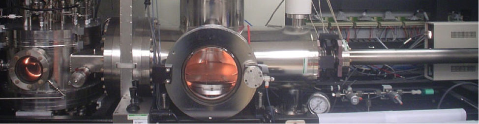
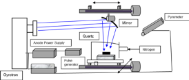
P-Type Conductivity and Damage Recovery in Implanted GaN Annealed by Rapid Gyrotron Microwave Annealing
V. Meyers, E. Rocco, T. J. Anderson, J. C. Gallagher, M. A. Ebrish, K. Jones, M. Derenge, M. Shevelev, V. Sklyar, K. Hogan, B. McEwen, and F. Shahedipour-Sandvik
Journal of Applied Physics, 128, 085701, 2020

Investigation of the Electrical Behavior of AlGaN/GaN High Electron Mobility Transistors Grown with Underlying GaN:Mg Layer
I. Mahaboob, S. W. Novak, E. Rocco, K. Hogan, and F. Shahedipour-Sandvik
Journal of Vacuum Science and Technology. B, 38, 062204, 2020

Synchrotron X-Ray Topography Characterization of High Quality Ammonothermal-Grown Gallium Nitride Substrates
Y. Liu, B. Raghothamachar, H. Peng, T. Ailihumaer, M. Dudley, R. Collazo, J. Tweedie, Z. Sitar, F. Shadi Shahedipour-Sandvik, K. A. Jones, A. Armstrong, A. A. Allerman, K. Grabianska, R. Kucharski, and M. Bockowski
Journal of Crystal Growth, 551, 125903, 2020

Drain-Voltage-Induced Secondary Effects in AlGaN/GaN HEMTs With Integrated Body-Diode
I. Mahaboob, M. Yakimov, E. Rocco, K. Hogan, and F. Shahedipour-Sandvik
IEEE Trans. Electron Devices, 67, 3983–3987, 2020

Removal of Dry-Etch-Induced Surface Layer Damage from p-GaN by Photoelectrochemical Etching
V. Meyers, E. Rocco, K. Hogan, S. Tozier, B. McEwen, I. Mahaboob, and F. Shahedipour-Sandvik
Journal of Electronic Materials, 49, 3481–3489, 2020

Hillock Assisted P-Type Enhancement in N-Polar GaN:Mg Films Grown by MOCVD
E. Rocco, O. Licata, I. Mahaboob, K. Hogan, S. Tozier, V. Meyers, B. McEwen, S. Novak, B. Mazumder, M. Reshchikov, L. Douglas Bell, and F. Shahedipour-Sandvik
Sci. Rep., 10, 1426, 2020

In Operando Investigation of GaN PIN Device Characteristics under Electron Irradiation Energies Comparable to Pm-147 Source for Betavoltaic Application
K. Hogan, M. Rodriguez, E. Rocco, V. Meyers, B. McEwen, and F. S. Shahedipour-Sandvik
AIP Advances, 10, 085110, 2020

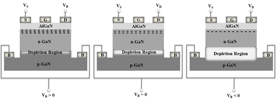
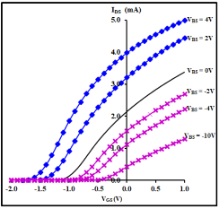
Dynamic Control of AlGaN/GaN HEMT Characteristics by Implementation of a p-GaN Body-Diode-Based Back-Gate
I. Mahaboob, M. Yakimov, K. Hogan, E. Rocco, S. Tozier, and F. Shahedipour-Sandvik
IEEE J. Electron Devices Soc., 7, 581–588, 2019

3D GaN-Based Betavoltaic Device Design with High Energy Transfer Efficiency
K. Hogan, M. Litz, and F. Shahedipour-Sandvik
Appl. Radiat. Isot., 145, 154–160, 2019

P-Type Conductivity and Suppression of Green Luminescence in Mg/N Co-Implanted GaN by Gyrotron Microwave Annealing
V. Meyers, E. Rocco, K. Hogan, B. McEwen, M. Shevelev, V. Sklyar, K. Jones, M. Derenge, and F. Shahedipour-Sandvik
Journal of Applied Physics, 130, 085704, 2021

Dopant-Defect Interactions in Mg-Doped GaN via Atom Probe Tomography
O. G. Licata, S. Broderick, E. Rocco, F. Shahedipour-Sandvik, and B. Mazumder
Appl. Phys. Lett., 119, 032102, 2021

Stability of the C N H i Complex and the Blue Luminescence Band in GaN
M. A. Reshchikov, O. Andrieiev, M. Vorobiov, B. McEwen, S. Shahedipour-Sandvik, D. Ye, and D. O. Demchenko
Phys. status solidi, 258, 2100392, 2021

Photoemission Characterization of N-Polar III-Nitride Photocathodes as Bright Electron Beam Source for Accelerator Applications
L. Cultrera, E. Rocco, F. Shahedipour-Sandvik, L. D. Bell, J. K. Bae, I. V. Bazarov, P. Saha, S. Karkare, and A. Arjunan
Journal of Applied Physics, 2021

Investigation of the Effects of Forming Gas Annealing on Al2O3/GaN Interface
B. McEwen, I. Mahaboob, E. Rocco, K. Hogan, V. Meyers, R. Green, F. Nouketcha, T. Murray, V. Kaushik, A. Lelis, and F. Shahedipour-Sandvik
Journal of Electronic Materials, 50, 80–84, 2021

Boronate Probe-Based Hydrogen Peroxide Detection with AlGaN/GaN HEMT Sensor
I. Mahaboob, R. J. Reinertsen, B. McEwen, K. Hogan, E. Rocco, J. A. Melendez, N. C. Cady, and F. Shahedipour-Sandvik
Exp. Biol. Med., 246, 523–528, 2021

Impurity Incorporation and Diffusion from Regrowth Interfaces in N-Polar GaN Photocathodes and the Impact on Quantum Efficiency
E. Rocco, I. Mahaboob, K. Hogan, V. Meyers, B. McEwen, L. D. Bell, and F. Shahedipour-Sandvik
Journal of Applied Physics, 129, 195701, 2021

P-Type Conductivity and Suppression of Green Luminescence in Mg/N Co-Implanted GaN by Gyrotron Microwave Annealing
V. Meyers, E. Rocco, K. Hogan, B. McEwen, M. Shevelev, V. Sklyar, K. Jones, M. Derenge, and F. Shahedipour-Sandvik
Journal of Applied Physics, 130, 085704, 2021

Polarization Engineered N-polar Cs-free GaN Photocathodes
J. Marini; I. Mahaboob; L.D. Bell; F. Shahedipour-Sandvik
J. Applied Physics, 124, 113101, 2018

Mg Incorporation Efficiency in Pulsed MOCVD of N-polar GaN:Mg
J. Marini; I. Mahaboob; K. Hogan; S. Novak; L.D. Bell; F. Shahedipour-Sandvik
Journal of Electronic Materials (Submitted)

Selective area epitaxial growth of stretchable geometry AlGaN-GaN heterostructures
I. Mahaboob, J.Marini, K. Hogan, E.Rocco, F. Shahedipour-Sandvik, R. P. Tompkins, and N. Lazarus
J. Electronic Materials, 47, 6625, 2018

(Editor Pick) Monte Carlo simulation of III-nitride photocathodes
J. Marini; L.D. Bell; F. Shahedipour-Sandvik
Journal of Applied Physics 123, 124502, 2018

Influence of mask material on the electrical properties of selective area epitaxy GaN microstructures
I. Mahaboob, K. Hogan, S. W. Novak, F. Shahedipour-Sandvik, R. P. Tompkins, N. Lazarus
Journal of Vacuum Science and Technology. B, 36, May 2018

A-plane GaN epitaxial lateral overgrowth structures: growth domains, morphological defects, and impurity incorporation directly imaged by cathodoluminescence microscopy
K. Hogan, S. Metzner, F. Bertram, I. Mahaboob, E. Rocco, F. Shahedipour-Sandvik, A. Dempewolf, J. Christen
Proc. SPIE 10532, Gallium Nitride Materials and Devices XIII, 105320V, 2018

Design and characterization of GaN p-i-n diodes for betavoltaic devices
Muhammad R.Khan, Joshua R.Smith, Randy P. Tompkins, Stephen Kelley, Marc Litz, John Russo, Jeff Leathersich, Fatemeh (Shadi) Shahedipour-Sandvik, Kenneth A.Jones, Agis Iliadis
Solid-State Electronics, 136, 24-29 (2017)

Electrical properties of AlGaN/GaN HEMTs in stretchable geometries
R. P. Tompkins, I. Mahaboob, S. Shahedipour-Sandvik, and N. Lazarus
Solid-State Electronics 136, 36-42, 2017

Mg Incorporation Efficiency in Pulsed MOCVD of N-polar GaN:Mg
J. Marini; I. Mahaboob; K. Hogan; S. Novak; L.D. Bell; F. Shahedipour-Sandvik
Journal of Electronic Materials, Vol. 46, No. 10, 2017

Mechanical Analysis of Stretchable AlGaN/GaN High Electron Mobility Transistors
R. P. Tompkins, I. Mahaboob, S. Shahedipour-Sandvik, and N. Lazarus
ECS Trans., 72(89), May 2016

MOCVD growth of N-polar GaN on on-axis sapphire substrate: impact of AlN nucleation layer on GaN surface hillock density
J. Marini; J. Leathersich; I. Mahaboob; J. Bulmer; N. Newman; F. Shahedipour-Sandvik
Journal of Crystal Growth 442 (2016)

Single Photon Counting UV Solar-Blind Detectors using Silicon and III-Nitride Materials
S. Nikzad; M. Hoenk; A. Jewell; J. Hennessy; A. Carver; T. Jones; T. Goodsall; E. Hamden; P. Suvarna; J. Bulmer; F. Shahedipour-Sandvik; E. Charbon; P. Padmanabhan; B. Hancock; L.D. Bell
Sensors 16, 927 (2016)

Surface photovoltage studies of p-type AlGaN layers after reactive-ion etching
J.D. McNamara; K.L. Phumisithikul; A.A. Baski; J. Marini; F. Shahedipour-Sandvik; S. Das; M.A. Reshchikov
Journal of Applied Physics 120, 155304 (2016)

Visible-Blind Avalanche Photodetector heterostructure Device Design with Superior Field Confinement and Low Operating Voltage
J. Bulmer; P. Suvarna; J.M. Leathersich; J. Marini; I. Mahaboob; N. Newman; F. Shahedipour-Sandvik
IEEE Photonics Technology Letters 28, 39-42 (2015)

(Invited) AlGaN films and the devices where they are utilized
K. A. Jones, T. P. Chow, M. Wraback, M. Shatalov, Z. Sitar, F. Shahedipour, K. Udwary, G. S. Tompa
Journal of Materials Research, 50, 3267 (2015).

Avalanche Photodiodes via Atomic Layer Deposition
J. Hennessy; L. D. Bell; S. Nikzad; P. Suvarna; F. Shahedipour-Sandvik
NASA Tech Brief 38, 12 (2014)

Ion implantation based edge termination to improve III-nitride APD reliability and performance
P. Suvarna; J. Bulmer; J.M. Leathersich; J. Marini; I. Mahaboob; J. Hennessy; L.D. Bell; S. Nikzard; F. Shahedipour-Sandvik
IEEE Photonics Technology Letters 27(5) (2015)

Tunable thermal quenching of photoluminescence in GaN
M. Reshchikov; J. McNamara; F. Shahedipour-Sandvik
Physica Status Solidi (c) 11, 389-392 (2014)

GaN Power Schottky Diodes with Drift Layers Growth on Four Substrates
R.P. Tompkins; J.R. Smith; K.W. Kirchner; J. Leach; K. Udwary; E. Preble; P. Suvarna; J. Leathersich; F. Shahedipour-Sandvik
Journal of Electronic Materials 43, 850-855 (2014)

Study of thermal stability of distributed Bragg reflectors based on epitaxial rare-earth oxide and silicon heterostructures
R. Dargis; J.M. Leathersich; F. Shahedipour-Sandvik; E. Arkun; A. Clark
Journal of Vacuum Science and Technology B 32, 02C103 (2014)

Annealing Studies of AlN Capped, MOCVD Grown GaN Films
M. A. Derenge, K. W. Kirchner, K. A. Jones, P. Suvarna; F. Shahedipour-Sandvik
Solid State Electronics, accepted-in press (2014).

(Invited) AlGaN films and the devices where they are utilized.
K. A. Jones, R. Tompkins, J. Leathersich, P. Suvarna, F. Shahedipour-Sandvik
Journal of Materials Research, submitted (2014).

Atomic-layer deposition for improved performance of III-N Avalanche photodiodes.
J. Hennessy, L. D. Bell, S. Nikzad, P. Suvarna, J. Leathersich, J. Marini, F. Shahedipour-Sandvik
Journal of Vacuum Science and Technology, submitted (2014).

ALD sidewall passivation for p-i-n Avalanche photodiodes.
J. Hennessey, L. D. Bell, S. Nikzad, P. Suvarna, F. Shahedipour-Sandvik
Journal of Applied Physics, submitted (2014).

The influence of buffer layer coalescence on stress evolution in GaN grown on ion implanted AlN/Si (111) substrates.
J. C. Gagnon,, J. M. Leathersich, F. S. Shahedipour-Sandvik, & J. M. Redwing
(2014) Journal of Crystal Growth, 393, 98-102.

Deposition of GaN films on crystalline rare earth oxides by MOCVD
J. Leathersich, E. Arkun, A. Clark, P. Suvarna, J. Marini, R. Dargis, F. Shehedipour-Sandvik, J. of Crystal Growth
accepted-in press (2014).

(Invited) Enhanced performance of AlGaN/GaN high electron mobility transistor on Si by means of improved adatom diffusion length during MOCVD epitaxy
F. Shahedipour-Sandvik, J. Leathersich, R.P. Tompkins, P. Suvarna, M. Tungare, T.A. Walsh, K. W. Kirchner, S. Zhou, and K. A. Jones
Semiconductor Science & Technology, 28, 074002 (2013).

Hybrid n-GaN and polymer interface: model systems for tunable photodiodes
P. Kumar, S. Guha, F. Shahedipour-Sandvik, and K. S. Narayan
Organic Electronics, 14, 2818 (2013).

Modification of dislocation behavior in GaN overgrown on engineered AlN thin film-on- bulk Si substrate
M. Tungare, X. Weng, J. M. Leathersich, P. Suvarna, J. Redwing, and F. Shahedipour-Sandvik
Journal of Applied Physics, 113, 163108 (2013).

Homoepitaxial growth of non-polar AlN crystals using Molecular Dynamics simulations
J. A. Leathersich, M. Tungare, P. Suvarna, F. Shahedipour-Sandvik,
Surface Science, 617, 36 (2013).

Growth of GaN by MOCVD on Rare Earth Oxide on Si(111)
F. Erdem Arkun, Rytis Dargis, Andrew Clark, Robin S. Smith, Michael Lebby, Jeffrey M. Leathersich, F. Shahedipour-Sandvik
Electrochem. Soc. Conference Proc. (2013).

Ion-Implantation-Induced Damage Characteristics Within AlN and Si for GaN-on-Si Epitaxy
J. Leathersich, M. Tungare, M. Evans, P. Suvarna, F. Shahedipour-Sandvik,
Journal of Electronic Materials, 42, 833 (2013).

Design and Growth of Visible-Blind and Solar-Blind III-N APDs on Sapphire Substrates
Puneet Suvarna, L. Douglas Bell, Mihir Tungare, Jeffrey M. Leathersich, Pratik Agnihotri, Shouleh Nikzad, F. (Shadi) Shahedipour-Sandvik
Journal of Electronic Materials, 42, 854 (2013).

HVPE GaN for high power electronic Schottky diodes
Randy P. Tompkins, Timothy A. Walsh, Michael A. Derenge, Kevin W. Kirchner, Shuai Zhou, Cuong B. Nguyen, Kenneth A. Jones, Gregory Mulholland, Robert Metzger, Jacob H. Leach, Puneet Suvarna, Mihir Tungare, and Fatemeh (Shadi) Shahedipour-Sandvik
Solid State Electronics 79, 238 (2013).

In situ stress measurements during GaN growth on ion-implanted AlN/Si substrates
J. C. Gagnon, M. Tungare, X. Weng, J. M. Leathersich, F. Shahedipour-Sandvik, J. M. Redwing
Journal of Electronic Materials 41, 865 (2012).

III-Nitride devices on Si: Challenges and opportunities
F. Shahedipour-Sandvik, M. Tungare, J. Leathersich, Suvarna, R. Tompkins, K. A. Jones,
Semicond. Dev. Res. Symp. (ISDRS), College Park, MD, (2011). DOI: 10.1109/ISDRS.2011.6135260. (2012)

Development of small unit cell avalanche photodiodes for UV imaging applications
A. K. Sood, R. E. Welser, R. A. Richwine, Y. R. Puri, R. D. Dupuis, J.-H. Ryou, N. K. Dhar, P. Suvarna, & F. Shahedipour-Sandvik.
SPIE Proc. 8375, Advanced Photon Counting Techniques VI, 83750R (2012).

A Tersoff-based interatomic potential for wurtzite AlN
M. Tungare, Y. Shi, N. Tripathi, P. Suvarna and F. Shahedipour-Sandvik
Physica Status Solidi (A): Applications and Materials Science 208, 1569 (2011).

Dielectric properties and thickness metrology of strain engineered GaN/AlN/Si (111) thin films grown by MOCVD
M. Tungare, V. K. Kamineni, F. Shahedipour-Sandvik, A. C. Diebold
Thin Solid Films 519, 2929 (2011).

AlGaN based III-nitride tunnel barrier hyperspectral detector: Effect of internal polarization
N. Tripathi, L. D. Bell, and F. Shahedipour-Sandvik
Journal of Applied Physics, 109 (2011).

(Invited) The effect of carbon impurities on lightly doped MOCVD GaN Schottky diodes
R. P. Tompkins, T. A. Walsh, M. A. Derenge, K. W. Kirchner, S. Zhou, C. B. Nguyen, K. A. Jones, P. Suvarna, M. Tungare, N. Tripathi, and F. Shahedipour-Sandvik
Journal of Materials Research 26, 2895 (2011).

AlGaN based III-nitride tunnel barrier hyperspectral detector for infrared detection
Shahedipour-Sandvik, F., Tripathi, N. & Bell, L. D.
Proceedings of SPIE - The International Society for Optical Engineering, 8155 (2011).

AlGaN based III-nitride tunnel barrier hyperspectral detector: Effect of internal polarization
Tripathi, N.; Bell, L. D.; Shahedipour-Sandvik, F.
Journal of Applied Physics 109, 124508 (2011)

Direct attachment of DNA to semiconducting surfaces for biosensor applications
N. M. Fahrenkopf, F. Shahedipour-Sandvik, N. Tokranova, M. Bergkvist, and N. C. Cady
Journal of Biotechnology, 150, 312 (2010).

Novel Cs-Free GaN Photocathodes
N. Tripathi, L.D. Bell, S. Nikzad, M. Tungare, P. Suvarna, and F. Shahedipour-Sandvik,
Journal of Electronic Materials, 40, 382 (2011).

Effect of n+ GaN cap polarization field on Cs-free GaN photocathodes characteristics
N. Tripathi, L. D. Bell, S. Nikzad, and F. Shahedipour-Sandvik,
Applied Physics Letters, 97, 052107 (2010).

Turn-on voltage engineering and enhancement-mode operation of AlGaN/GaN high electron mobility transistor using multiple heterointerfaces
N. Tripathi, V. Jindal, S. Rajan, A. Vert, and F. Shahedipour-Sandvik,
Solid State Electronics, 54, 1291 (2010).

Computational and experimental studies on the growth of non-polar surfaces of gallium nitride
V. Jindal, and F. Shahedipour-Sandvik,
Journal of Applied Physics, 107, 054907 (2010).

Theoretical prediction of GaN nanostructure equilibrium and non-equlibrium shapes
V. Jindal, and F. Shahedipour-Sandvik,
Journal of Applied Physics, 106, 083115 (2009).

Defect-related photoluminescence in Mg-doped GaN nanostructures
M. A. Reshchikov, F. Shahedipour-Sandvik, B. J. Messer, V. Jindal, N. Tripathi, and M. Tungare,
Physics B: Condensed Matter, 404, 4903 (2009).

Direct mobilization and hybridization of DNA on group III-nitride semiconductors
Xiabin Xu, V. Jindal, F. Shahedipour-Sandvik, M. Berkvitz, and N. Cady,
Applied Surface Science, 225, 5905 (2009).

Density functional theoretical study of surface structure and adatom kinetics for wurtzite AlN
V. Jindal, and F. Shahedipour-Sandvik,
Journal of Applied Physics, 105, 084902 (2009).

Density functional calculations of the strain effects on binding energies and adatom diffusion on (0001) GaN surfaces
J. R. Grandusky, V. Jindal, J. Reynolds, and F. Shahedipour-Sandvik,
Materials Science and Engineering B: Solid-state materials for advanced technology,158, 13 (2009).

III-nitride heterostructure layered tunnel barriers for a tunable hyperspectral detector
Bell, L. Douglas; Tripathi, Neeraj; Grandusky, J. R.; Jindal, Vibhu; Shahedipour-Sandvik, F. Shadi
IEEE Sensors Journal 8, 724-729 (2008)

Fully Tunable Hyperspectral Imaging Detector based on III-Nitride Dielectric Heterostructures
L. D. Bell, N. Tripathi, J. R. Grandusky, V. Jindal, and F. Shahedipour-Sandvik,
IEEE Sensors J., special issue on “Nanosensors for Defense and Security”, 8, 724 (2008).

Selective area heteroepitaxy of low dimensional a-plane and c-plane InGaN nanostructures using pulsed MOCVD
V. Jindal, N. Tripathi, M. Tungare, O. Pachos, P. Haldar, and F. Shahedipour-Sandvik,
Physica Status Solidi (c), 5, 1709 (2008).

Growth and characterization of a novel hyperspectral detector using the III-nitrides
N. Tripathi, L. D. Bell, J. R. Grandusky, V. Jindal, and F. Shahedipour-Sandvik,
Physica Status Solidi (c), 5, 2228 (2008).

Effect of interfacial strain on AlGaN hexagonal nanostructures by selective area heteroepitaxy
V. Jindal, J. R. Grandusky, N. Tripathi, B. Thiel, and F. Shahedipour-Sandvik,
Physica E: low dimensional systems and nanostructure, 40, 478 (2008).

Identification of subsurface damage in freestanding HVPE GaN substrates and its influence on epitaxial growth of GaN epilayers
Grandusky, J. R.; Jindal, V.; Tripathi, N.; Shahedipour-Sandvik, F.; Lu, H.; Kaminsky, E. B.; Melkote, R.
Journal of Crystal Growth 307, 309-314 (2007)

AlGaN based Tunable Hyperspectral Detector
N. Tripathi, J. Grandusky, V. Jindal, F. Shahedipour-Sandvik, and L. D. Bell,
Applied Physics Letter 90, 231103 (2007).

Identification of important growth parameters for the development of high quality Al>0.5GaN by MOCVD
J. R. Grandusky, M. Jamil, V. Jindal, N. Tripathi, and F. Shahedipour-Sandvik,
J. Vacuum Science and Technology A, 25(3), (2007).

Homoepitaxial growth and electrical characterization of GaN-based Schottky and light-emitting diodes
X. A. Cao, H. Lu, E. B. Kaminsky, S. D. Arthur, J. R. Grandusky, and F. Shahedipour-Sandvik,
J. Crystal Growth, 300, 382, (2007).

Mechanism of large area dislocation reduction in GaN layers on AlN/Si (111) by substrate engineering
M. Jamil, J. R. Grandusky, V. Jindal, N. Tripathi, and F. Shahedipour-Sandvik,
J. Applied Physics 102, 023701 (2007); Virtual Journal of Nanoscale Science & Technology, 16, 5 (2007).

Selective area heteroepitaxy of nano-AlGaN UV excitation sources for bioflourescence application
V. Jindal, J. R. Grandusky, F. Shahedipour-Sandvik, S. F. LeBouef, J. Balch, and T. Tolliver,
“Outstanding MRS Paper Award”, J. Materials Research 22, 838, (2007).

High resolution x-ray diffraction analyses of ion-implanted GaN/AlN/Si heterostructures
R. J. Matyi, M. Jamil, and F. Shahedipour-Sandvik,
Physica Status Solidi A, 204, 2598 (2007).

Development of pit-defect free smooth a-plane GaN surfaces on r-plane sapphire using MOCVD: A growth mechanism study
V. Jindal, J. Grandusky, M. Jamil, E. Irissou, F. Shahedipour-Sandvik, K. Matocha, and V. Tilak,
Physica Status Solidi (a) 3, 179, (2006).

Reduction of crack and dislocation defects in GaN layers grown on Si substrate by MOCVD using a substrate engineering technique
M. Jamil, E. Irissou, J. R. Grandusky, V. Jindal, and F. Shahedipour-Sandvik,
Physica Status Solidi (c) 3, 1787, (2006).

Development of native, single crystal AlN substrates for device applications
L. J. Schowalter, S. B. Schujman, W. Liu, M. Goorsky, M. C. Wood, J. Grandusky, and F. Shahedipour-Sandvik,
Physica Status Solidi (a) 203, 1667 (2006).

Origin of ring defects in high In content green InGaN/GaN MQW: An Ultrasonic Force Microscopy Study
F. Shahedipour-Sandvik, M. Jamil, K.Topol, J. R. Grandusky, K. A. Dunn, J. Ramer, and V. N. Merai,
MRS Internet J. Nitride Semiconductor Research 10, 3 (2005).

Deep green emission at 570nm from InGaN/GaN MQW active region grown on bulk AlN substrate
F. Shahedipour-Sandvik, J. R. Grandusky, M. Jamil, V. Jindal, S. B. Schujman, L. J. Schowalter, R. Liu, F. A. Ponce, M. Cheung, A. Cartwright
International Society for Optical Engineering, 5941, 37 (2005).

Development of Strain Reduced GaN on Si(111) by Substrate Engineering
M. Jamil, J. R. Grandusky, V. Jindal, S. Guha, A. Arif, and F. Shahedipour-Sandvik,
Applied Physics Letters 87, 82103 (2005).

Optimization of the active region of InGaN/GaN 405 nm light emitting diodes using statistical design of experiments for determination of interaction effects
J. R. Grandusky, M. Jamil, J. A. Deluca, S. F. LeBoeuf, X. A. Cao, S. D. Arthur, and F. Shahedipour-Sandvik,
J. Vacuum Science and Technology B 23, 1576 (2005).

Development of low dislocation and strain reduced GaN on Si(111) by substrate engineering
M. Jamil, J. R. Grandusky, V. Jindal, F. Shahedipour-Sandvik, S. Guha, M. Arif
International Society for Optical Engineering, 5941, 59411 (2005).

Important interaction effects in the growth of InGaN violet light emitting diodes by MOCVD
J. R. Grandusky, M. Jamil, V. Jindal, J. A. DeLuca, S. F. LeBoeuf, X. A. Cao, S. D. Arthur, F. Shahedipour-Sandvik
International Society for Optical Engineering, 5941, 144 (2005).

Strain dependent facet stabilization in selective area heteroepitaxial growth of GaN nanostructures
F. Shahedipour-Sandvik, J. R. Grandusky, A. Alizadeh, C. Keimel, S. Taylor, S. LeBoeuf, S. Ganthi, and P. Sharma,
Applied Physics Letters 87, 233108 (2005).
Virtual Journal of Nanoscale Science & Technology, 12, 24 (2005)

Microstructural origin of leakage current in GaN/InGaN Light Emitting Diodes
X. A. Cao, J. Teetsov, F. Shahedipour-Sandvik, and S. D. Arthur,
J. Crystal Growth, 264, 172 (2004).

Influence of defects on electrical and optical characteristics of GaN/InGaN-based light-emitting diodes
Xian-an Cao, K. Topol, F. Shahedipour-Sandvik, J. Teetsov, Peter M. Sandvik, Stephen E. LeBoeuf, Abasifreke Ebong, James W. Kretchmer, Edward B. Stokes, S. Arthur, Alain E. Kaloyeros, D. Walker,
International Society for Optical Engineering, 4776, 105 (2002).

Efficient GaN Photocathodes for Low-Level Ultra-Violet Signal Detection
F. Shahedipour, B. W. Wessels, M. P. Ulmer, C. Josef, and T. Nihashi,
IEEE J. of Quantum Electronics 38, 333 (2002).

Defects observed by optical detection of electron paramagnetic in electron-irradiated p-type GaN
L. S. Vlasenko, C. Bozdog, G. D. Watkins, F. Shahedipour and B. W. Wessels
Physica Review B 65, 205202 (2002).

AlxGa1-xN for Solar-Blind UV Photodetectors
P. Sandvik, K. Mi, F. Shahedipour, P. Kung, R. McClintock, A. Yasan, and M. Razeghi
J. of Crystal growth 231, 366 (2001).

Comparative Optical Studies of p-type and unintentionally doped GaN: The Influence of annealing
S. Guha, F. Shahedipour, R.C. Keller, V. Yang and B.W. Wessels
Applied Physics Letters 78, 58 (2001).

Progress in the fabrication of GaN photocathodes
Melville P. Ulmer, Bruce W. Wessels, Fatemeh Shahedipour, Roman Y. Korotokov, Charles L. Joseph, Tokuaki Nihashi,
International Society for Optical Engineering, 4288, 246 (2001).

On the origin of the 2.8 eV blue emission in p-type GaN:Mg: A time-resolved photoluminescence investigation
F. Shahedipour and B. W. Wessels
MRS Internet J. Nitride Semiconductor Research 6, 12 (2001).

AlxGa1-xN materials and device technology for solar blind ultraviolet photodetector applications
Ryan McClintock, Peter M. Sandvik, Kan Mi, Fatemeh Shahedipour, Alireza Yasan, Christopher L. Jelen, Patrick Kung, Manijeh Razeghi,
International Society for Optical Engineering, 4288, 219 (2001).

Solar-blind AlxGa1-xN p-i-n photodetectors grown on LEO and non-LEO GaN
Peter M. Sandvik, Danielle Walker, Patrick Kung, Kan Mi, Fatemeh Shahedipour, Vipan Kumar, Xinghong Zhang, Jacqueline E. Diaz, Christopher L. Jelen, Manijeh Razeghi,I
nternational Society for Optical Engineering, 3948, 265 (2000).

Lateral Epitaxial Overgrowth of GaN on Sapphire and Silicon Substrates for Ultraviolet Photodetector Applications
M. Razeghi, P. Sandvik, P. Kung, D. Walker, K. Mi, X. Zhang, V. Kumar, J. Diaz and F. Shahedipour
Materials Science and Engineering B 74, 107 (2000).

Investigation of the formation of the 2.8 eV luminescence band in p-type GaN:Mg:
F. Shahedipour, and B. W. Wessels
Applied Physics Letters 76, 3011 (2000).

Photoluminescence Band Near 2.9 eV in Undoped GaN Epitaxial Layers
M. A. Reshchikov, F. Shahedipour, R. Y. Korotkov, and B. W. Wessels
J. Applied Physics, 87, 3351 (2000).

Pressure Dependence of the Blue Luminescence in Mg doped GaN
S. Ves, U. D. Venkateswaran, I. Loa, K. Syassen, F. Shahedipour, B. W. Wessels
Applied Physics Letters, 77, 2536 (2000).

Optical Properties of Plasma Species Adsorbed during Diamond Deposition on Steel
F. Shahedipour, B. P. Conner, and H. W. White,
J. Applied Physics, 88, 3039 (2000).

Deep Acceptors in Undoped GaN
M. A. Reshchikov, F. Shahedipour, R.Y. Korotkov, M.P. Ulmer, and B. W. Wessels,
Physica B 273-274, 105 (1999).

Low Temperature Synthesis of Diamond-like Carbon Film on Steel Substrates by ECR-PACVD
S. Zhu, F. Shahedipour, and H. W. White,
J. American Ceramic Society, 81, 1041 (1998).

Evidence of Apical Oxygen in Artificially Superconducting SrCuO2- BaCuO2 Thin Films: A Raman Characterization.
S. Zhu, D. P. Norton, J. E. Chamberlin, F. Shahedipour, and H.W. White,
Physical Review B, 54, 1 (1996).

Conference Proceeding Articles

E. Rocco, I. Mahabob, K. Hogan, S. Tozier, V. Meyers, B. McEwen, S. Novak, B. Mazumder, L.D. Bell, F. Shahedipour-Sandvik
Enhanced p-type conductivity in N-polar GaN photocathode structures and correlation with GaN hillock density
Proc. SPIE, Gallium Nitride Materials and Devices XIV, 10918, 2019

Impact of Interface Properties in N-polar Heterostructure GaN Photocathodes
E. Rocco; I. Mahaboob; K. Hogan; V. Meyers; S. Tozier; L.D. Bell; F. Shahedipour-Sandvik
Electronic Materials Conference, University of California Santa Barbara (2018)

Influence of Mask Material in Controlling the Electrical Properties of Selective Area Epitaxially Grown AlGaN-GaN Microstructures
I. Mahaboob; K. Hogan; E. Rocco; R. Tompkins; N. Lazarus; F. Shahedipour-Sandvik
Electronic Materials Conference, University of California Santa Barbara (2018)

Progress in Cesium-Free III-Nitride Photocathodes Based on Control of Polarization Charge
L.D. Bell; E. Rocco; J. Marini; S. Nikzad; F. Shahedipour-Sandvik
American Physical Society March Meeting, Los Angeles, California (2018)

Design and Bottom-Up Development of Stretchable Geometry AlGaN/GaN High Electron Mobility Transistors
I. Mahaboob; J. Marini; K. Hogan; E. Rocco; R. Tompkins; N. Lazarus; F. Shahedipour-Sandvik
Electronic Materials Conference, University of Notre Dame (2017)

Impact of Al Composition of AlxGa1-xN Alloys and GaN Polarity on Thermoelectric Properties of III-Nitrides
S. Tozier; M. Rivera; I. Mahaboob; K. Hogan; E. Rocco; J. Marini; F. Shahedipour-Sandvik
Electronic Materials Conference, University of Notre Dame (2017)

Investigation of Surface Treatments for Improved Quantum Efficiency in III-N Photocathodes
E. Rocco; J. Marini; I. Mahaboob; K. Hogan; J.D. McNamara; M.A. Reshchikov; L.D. Bell; F. Shahedipour-Sandvik
Electronic Materials Conference, University of Notre Dame (2017)

Monte Carlo Simulation of III-Nitride Photocathodes
J. Marini; I. Mahaboob; K. Hogan; E. Rocco; L.D. Bell; F. Shahedipour-Sandvik
Electronic Materials Conference, University of Notre Dame (2017)

Towards High Performance (Al)GaN Based Betavoltaic Device
K. Hogan; J. Marini; I. Mahaboob; E. Rocco; F. Shahedipour-Sandvik
Electronic Materials Conference, University of Notre Dame (2017)

Development of Stretchable Geometry AlGaN/GaN HEMTs with Selective Area Epitaxial Growth Technique
I. Mahaboob; J. Marini; K. Hogan; R.P. Tompkins; N. Lazarus; F. Shahedipour-Sandvik
International Workshop on Nitride Semiconductors, Orlando (2016)

Optimization of (Al)GaN Based Betavoltaic Device
K. Hogan; J. Marini; I. Mahaboob; F. Shahedipour-Sandvik
International Workshop on Nitride Semiconductors, Orlando (2016)

Mg dopant incorporation efficiency in pulsed MOCVD Growth of N-polar p-GaN
J. Marini; I. Mahaboob; K. Hogan; S. Novak; L.D. Bell; S. Nikzad; F. Shahedipour-Sandvik
Electronic Materials Conference, University of Delaware (2016)

Thermoelectric Properties of III-Nitrides Single Layer and Heterojunctions
S. Tozier; I. Mahaboob; S. Chakraborty; N. Newman; J. Marini; F. Shahedipour-Sandvik
Electronic Materials Conference, University of Delaware (2016)

Impact of Mg-Doping on the Stress Evolution in GaN Epitaxy on Si Substrate
J. Leathersich; I. Mahaboob; J. Marini; J. Bulmer; N. Newman; F. Shahedipour-Sandvik
Electronic Materials Conference, University of Delaware (2016)

Stress Modification and Surface Morphology Improvement in Epitaxially Grown a-plane GaN Using Indium Surfactant
N. Newman; J. Marini; I. Mahaboob; K. Hogan; D. Anderson; R. Hull; F. Shahedipour-Sandvik
Electronic Materials Conference, University of Delaware (2016)

Performance Enhancement in AlGaN/GaN HEMT Characteristics with the Implementation of Dynamic Body Bias Technique
I. Mahaboob; J. Leathersich; J. Marini; J. Bulmer; N. Newman; F. Shahedipour-Sandvik
Materials Research Society Fall Meeting, Boston (2015)

Challenges for Solar-Blind III-Nitride based Photocathodes
J. Marini; J. Leathersich; I. Mahaboob; J. Bulmer; N. Newman; L.D. Bell; S. Nikzad; J. Hennessy; F. Shahedipour-Sandvik
Electronic Materials Conference, Ohio State University (2015)

Impact of Dopant Species on Lateral Overgrowth of GaN by Pulsed MOCVD on Chemically Treated Core Shell GaN on Silicon
N. Newman; M. Kotha; J. Leathersich; J. Marini; I. Mahaboob; J. Bulmer; F. Shahedipour-Sandvik; R. Debnath; A. Motayed
Electronic Materials Conference, Ohio State University (2015)

GaN Based P-i-N Devices for Betavoltaic Microbatteries
M.R. Khan; J.R. Smith; S. Kelley; K. Kirchner; R.P. Tompkins; I. Mahaboob; J. Leathersich; J. Marini; P. Suvarna; F. Shahedipour-Sandvik; K.A. Jones; A. Iliadis
Electronic Materials Conference, Ohio State University (2015)

Implementation of Dynamic Body-Bias Technique in AlGaN/GaN High Electron Mobility Transistors (HEMTs)
I. Mahaboob; J. Leathersich; J. Marini; J. Bulmer; N. Newman; F. Shahedipour-Sandvik
Electronic Materials Conference, Ohio State University (2015)

Atomic-layer deposition for improved performance of III-N Avalanche Photodiodes
J. Hennessy, L. D. Bell, S. Nikzad, P. Suvarna, J. Leathersich, J. Marini, F. Shahedipour-Sandvik
Materials Research Society Symposiym Proceeding (2014)

Crack-free III-nitride structures (> 3.5 µm) on silicon
M. Tungar, J. M. Leathersich, N. Tripathi, P. Suvarna, F. Shahedipour-Sandvik, T. A. Walsh, R. P. Tompkins, and K. A. Jones,
Materials Research Society Symposium Proceedings 1324, 9 (2012).

III-Nitride devices on Si: Challenges and opportunities
F. Shahedipour-Sandvik; M. Tungare; J. Leathersich; P. Suvarna; R. Tompkins; K.A. Jones
Semiconductor Device Research Symposium (ISDRS) (2012)

Development of small unit cell avalance photodiodes for UV imaging applications
Sood, A.K.; Welser, R.E.; Richwine, R.A.; Puri, Y.R.; Dupuis, R.D.; Ryou, J.-H.; Dhar, N.K.; Suvarna, P.; Shahedipour-Sandvik, F.
Proceedings of SPIE 8375, Advanced Photon Counting Techniques VI, 83750R (2012)

Materials Research Society Symposium Proceedings: Preface
Bell, L.D.; Shahedipour-Sandvik, F.; Jones, K.A.; Schaadt, D.; Simpkins, B.S.; Contreras, M.A.
Materials Research Society Symposium Proceedings 1324, ix-x (2012)

Crack-free III-nitride structures (>3.5&u;m) on silicon
M. Tungare; J.M. Leathersich; N. Tripathi; P. Suvarna; F. Shahedipour-Sandvik; T.A. Walsh; R.P. Tompkins; K.A. Jones Materials Research Society Symposium Proceedings 1324, 9-15 (2012)

AlGaN based III-nitride tunnel barrier hyperspectral detector for infrared detection
Shahedipour-Sandvik, F.; Tripathi, N.; Bell, L.D.
Proceedings of SPIE 5155, 81550P (2011)

A III-nitride Layered Barrier Structure for Hyperspectral Imaging Applications
Douglas Bell, Neeraj Tripathi, James Grandusky, Vibhu Jindal and Fatemeh Shahedipour-Sandvik.
Materials Research Society Symposium Proceedings, 1167 (2009).

Exploiting Phosphate Dependent DNA Immobilization on HfO2, ZrO2 and AlGaN for Integrated Biosensors
Nicholas M Fahrenkopf, Vibhu Jindal, Neeraj Tripathi, Serge Oktyabrsky, Fatemeh Shahedipour-Sandvik, Natalya Tokranova, Magnus Bergkvist and Nathaniel C Cady
Materials Research Society Symposium Proceedings 1236 (2009).

Effect of interfacial strain on shape and composition of MOCVD grown III-Nitride nanostructures
V. Jindal, J. R. Grandusky, N. Tripathi, M. Tungare, and F. Shahedipour-Sandvik,
Materials Research Society Symposium Proceedings ,1087 (2008).

Density functional calculations of the binding energies and adatom diffusion on strained AlN (0001) and GaN (0001) surface
V. Jindal, J. R. Grandusky, N. Tripathi, M. Tungare, and F. Shahedipour-Sandvik
Materials Research Society Symposium Proceedings, 1040 (2008).

Development of homoepitaxially grown GaN thin film layers on freestanding bulk m-plane substrates by metalorganic chemical vapor deposition (MOCVD)
V. Jindal, J. R. Grandusky, M. Tungare, N. Tripathi, F. Shahedipour-Sandvik, P. Sandvik, V. Tilak
Materials Research Society Symposium Proceedings, 1040 (2008).

Ultrafast carrier dynamics and recombination in green emitting InGaN MQW LED
A. N. Cartwright, M. Cheung, F. Shahedipour-Sandvik, J. R. Grandusky, M. Jamil, V. Jindal, C. Wetzel, P. Li, T. Dtchprohm, and J. Nelson
Materials Research Society Symposium Proceedings, 916, 7 (2006).

Selective area heteroepitaxy of nano-AlGaN UV excitation sources for bioflourescence application
V. Jindal, J. R. Grandusky, F. Shahedipour-Sandvik, S. F. LeBouef, J. Balch, and T. Tolliver
Materials Research Society Symposium Proceedings, 916, 97 (2006).

Effect of HVPE GaN substrate condition on the characteristics and performance of 405nm LEDs
J. R. Grandusky, M. Jamil, V. Jindal, F. Shahedipour-Sandvik, H. Lu, X._A. Cao, and E. B. Kaminsky
Materials Research Society Symposium Proceedings, 916, 91(2006).

Dislocation reduction and structural properties of GaN layers grown on N+implanted AlN/Si (111) substrates
M. Jamil, J. R. Grandusky, V. Jindal, N. Tripathi and F. Shahedipour-Sandvik
Materials Research Society Symposium Proceedings, 892 (2005).

Effects of GaN template annealing on the optical and morphological quality of the homoepitaxially overgrown GaN layer
James R. Grandusky, Vibhu Jindal, Muhammad Jamil and Fatemeh Shahedipour-Sandvik
Materials Research Society Symposium Proceedings, 892 (2005).

Deep green emission at 570nm from InGaN/GaN MQW active region grown on bulk AlN substrate
F. Shahedipour-Sandvik; J.R. Grandusky; M. Jamil; V. Jindal; S.B. Schujman; L.J. Schowalter; R. Liu; F.A. Ponce; M. Cheung; A. Cartwright
Proceedings of SPIE 5941, 594107 (2005)

Development of low dislocation and strain reduced GaN on Si(111) by substrate engineering
M. Jamil; J.R. Grandusky; V. Jindal; F. Shahedipour-Sandvik; S. Guha; M. Arif
Proceedings of SPIE 5941, 59411E (2005)

Important interaction effects in the growth of InGaN violet light emitting diodes by MOCVD
J.R. Grandusky; M. Jamil; V. Jindal; J.A. DeLuca; S.F. LeBoeuf; X.A. Cao; S.D. Arthur; F. Shahedipour-Sandvik
Proceedings of SPIE 5941, 59410W (2005)

Effect of GaN Surface Treatment on the Morphological and Optoelectronic properties of Violet Light Emitting Diodes
M. Jamil, J. R. Grandusky and F. Shahedipour-Sandvik
Materials Research Society Symposium Proceedings, 831 (2004).

Influence of defects on electrical and optical characteristics of GaN/InGaN-based light-emitting diodes
X.-A. Cao; K. Topol; F. Shahedipour-Sandvik; J. Teetsov; P.M. Sandvik; S.E. LeBoeuf; A. Ebong; J.W. Kretchmer; E.B. Stokes; S. Arthur; A.E. Kaloyeros; D. Walker
Proceedings of SPIE 4776, 105 (2002) doi: 10.1117/12.452581

Progress in the fabrication of GaN photocathodes
M.P. Ulmer; B.W. Wessels; F. Shahedipour; R.Y. Korotkov; C.L. Joseph; T. Nihashi
Proceedings of SPIE 4288, 246 (2001)

AlxGa1-xN materials and device technology for solar blind ultraviolet photodetector applications
R. McClintock; P.M. Sandvik; K. Mi; F. Shahedipour; A. Yasan; C.L. Jelen; P. Kung; M. Razeghi
Proceedings of SPIE 4288, 219 (2001)

Solar blind AlxGa1-xN p-i-n photodetectors grown on LEO and non-LEO GaN
P.M. Sandvik; D. Walker; P. Kung; K. Mi; F. Shahedipour; V. Kumar; X. Zhang; J.E. Diaz; C.L. Jelen; M. Razeghi
Proceedings of SPIE 4288, 265 (2001)

In Situ FTIR Spectroscopic Detection of Adsorbed Species on Sapphire Substrate in a Diamond ECR-PACVD System
F. Shahedipour, S. Zhu, and H. W. White,
Materials Research Society Symposium Proceedings, 502 (1998).

Determination of hydrogen in CVD diamond by notched neutron spectrum technique and FTIR
F. Golshani, W. H. Miller, M. A. Prelas, T. Sung, G. Popovici, G. Manning, S. K. Loyalka, F. Shahedipour. H. W. White, W. D. Brown, A. P. Malshe. and H. A. Naseem, Materials
Research Society Symposium Proceedings, 416, 361 (1996).

Growth and Characterization of Polycrystalline Diamond Films on Porous Silicon By Hot Filament CVD
S. Mirzakuchak, E.J. Charlson, E.M. Charlson, T. Stacy, F. Shahedipour, H. W. White
Materials Research Society Symposium Proceedings, 423 (1996).

Raman and FTIR Study of Neutron Irradiated CVD Diamond
S. Khasawinah, G. Popovici, M. A. Prelas, M. McCormick, S. K. Loyalka, G. Manning, J. Farmer, H. W. White, and F. Shahedipour
Materials Research Society Symposium Proceedings, 416, 223 (1996).

Conference Presentations

Toward Highly Efficient P-Doping in III-Nitride Optoelectronics: MOCVD Growth of Be-Doped GaN
B. McEwen, M. Reshchikov, E. Rocco, V. Meyers, K. Hogan, O. Andrieiev, M. Vorobiov, D. Demchenko, and S. Shahedipour-Sandvik
in Gallium Nitride Materials and Devices XVII, 2022, PC12001, 84

Microwave-Induced Annealing, Its Impact on Mg Diffusion and Photoluminescence Activity in Implanted and In Situ Doped GaN
V. Meyers, E. Rocco, K. Hogan, B. McEwen, M. A. Derenge, K. A. Jones, M. Shevelev, V. Sklyar, and F. Shahedipour-Sandvik
in 63rd Electronic Materials Conference, 2021, 151

AlGaN/GaN HEMT-Based Detection of Reactive Oxygen Species Molecule H2O2
I. Mahaboob, R. J. Reinertsen, B. McEwen, K. Hogan, E. Rocco, V. Meyers, J. A. Melendez, N. C. Cady, and F. Shahedipour-Sandvik
in 63rd Electronic Materials Conference, 2021, 91

(Invited) Defect Microstructural Evolution of Co-Implanted and Gyrotron Microwave-Annealed GaN
S. Shahedipour-Sandvik, V. Meyers, E. Rocco, K. Hogan, B. McEwen, M. Derenge, K. Jones, M. Shevelev, and V. Sklyar
in ECS Meeting Abstracts, 2021, MA2021-02, 998–998

Cs-Free N-Polar III-Nitride Photocathode Detectors with High Quantum Efficiency: Role of Impurity Incorporation at Interfaces and Planes
E. Rocco, K. Hogan, V. Meyers, B. McEwen, L. D. Bell, and F. S. Shahedipour-Sandvik
in Gallium Nitride Materials and Devices XVI, 2021, 11686, 34

In Operando Investigation of GaN PIN Device Characteristics under Electron Irradiation Energies Comparable to Pm-147 Source for Betavoltaic Application
K. Hogan, M. Rodriguez, E. Rocco, V. Meyers, B. McEwen, and F. Shahedipour-Sandvik
in 62nd Electronic Materials Conference, 2020, 94

Oxygen Impurity Incorporation Due to Growth Interruption and Its Diffusion from These Interfaces in N-Polar GaN:Mg Films Grown by MOCVD and Its Implication in Photocathode Device Characteristics
E. Rocco, K. Hogan, V. Meyers, B. McEwen, L. Douglas Bell, and F. Shahedipour-Sandvik
in 62nd Electronic Materials Conference, 2020, 64

Secondary Effects in Electrical Behavior of Body-Diode Integrated AlGaN/GaN HEMTS
I. Mahaboob, M. Yakimov, E. Rocco, K. Hogan, V. Meyers, and F. S. Shahedipour-Sandvik
in ECS Meeting Abstracts, 2020, MA2020-02, 3598–3598

V. Meyers et al. “P-type Conductivity in Mg-implanted GaN by Microwave Gyrotron Annealing”, 62nd Electronic Materials Conference June 2020

S. Shahedipour-Sandvik et al. Keynote, “Wide band-gap semiconductor power electronics”, 8th European Conference on Renewable Energy Systems, Istanbul, Turkey, June 2020

S. Shahedipour-Sandvik et al., Invited, “ECS 2020 title”, PRiME (ECS) Oct. 2020

V. Meyers et al. “P-Conductivity in Co-Implanted and Gyrotron Microwave-Annealed GaN: Optical and Electrical Studies”, PRiME (ECS), Oct. 2020

B. McEwen, I. Mahaboob, K. Hogan, E. Rocco, V. Meyers, S. Tozier, A. Lelis, R. Green, F. Nouketcha, F. Shahedipour-Sandvik
Effects of Forming Gas Anneal on the Structure of Al2O3/GaN Interface
The 61st Electronic Materials Conference, Ann Arbor, MI, 2019

B. McEwen, I. Mahaboob, K. Hogan, E. Rocco, V. Meyers, S. Tozier, A. Lelis, R. Green, F. Nouketcha, F. Shahedipour-Sandvik
Effects of Semiconductor Surface Treatments and Dielectric Anneal on the Electrical Characteristics of GaN based Metal-Insulator-Semiconductor Devices
MRS International Conference on Nitride Semiconductors, Bellevue, WA, 2019

I. Mahaboob, M. Yakimov, S. Tozier, K. Hogan, E. Rocco, F. Shahedipour-Sandvik
Integrated Body-Diode Back-Gate Control in AlGaN/GaN HEMTs
The 61st Electronic Materials Conference, Ann Arbor, MI, 2019

K. Hogan, S. Tozier, E. Rocco, I. Mahaboob, V. Meyers, B. McEwen, F. Shahedipour-Sandvik, R. Tompkins, M. Derenge, K. Jones, M. Shevelev, V. Sklyar, A. Lang, J. Hart, M. Taheri and M. Reshchikov
Novel Gyrotron Beam Annealing Method for Mg-Implanted Bulk GaN
2019 IEEE International Reliability Physics Symposium (IRPS), 2019

K. Hogan, S. Tozier, M. Graziano, M. Derenge, M. Shevelev, V. Sklyar, A.C. Lang, K. Jones, M.L. Taheri, W. Sung, and F. Shahedipour-Sandvik
Magnesium implant-activation in GaN: Impact of high temperature annealing techniques on the state of implant induced defects and Mg activation.
SPIE Photonics West, San Francisco, CA, 2019

K. Hogan, S. Tozier, E. Rocco, I. Mahaboob, V. Meyers, B. McEwen, F. Shahedipour-Sandvik, R. Tompkins, M. Derenge, K. Jones, M. Shevelev, V. Sklyar, A. Lang, J. Hart, M. Taheri and M. Reshchikov.
High Power GaN Devices: Novel Gyrotron Beam Annealing Method for Mg-Implanted Bulk GaN as an Enabling Technology.
The International Reliability Physics Symposium, Monterey, CA, 2019

S. Tozier, M. Reshchikov, K. Hogan, E. Rocco, V. Meyers, B. McEwen, I. Mahaboob, M. Shevelev, V. Sklyar, R. Tompkins, M. Derenge, A. Lang, K. Jones, M. Taheri, W. Sung and F. Shahedipour-Sandvik
Photoluminescence characterization of high temperature microwave annealed homoepitaxially grown Mg-implanted GaN.
The MRS Electronic Materials Conference, Ann Arbor, MI, 2019

K. Hogan, E. Rocco, S. Tozier, V. Meyers, M. Shevelev, V. Sklyar, R. Tompkins, M. Derenge, K. Jones, J. Hart, M. Taheri, W. Sung, and F. Shahedipour-Sandvik
Toward selective activation of Mg doped GaN: Impact of pulsed and continuous gyrotron annealing.
The MRS International Conference on Nitride Semiconductors, Bellevue, WA, 2019

F. Shahedipour-Sandvik
Impact of post implantation annealing on defect microstructural evolution in GaN:Mg.
Invited talk at the International Conference on Defects in Semiconductors, Seattle, WA, 2019

K. Hogan, J. Russo, M. Litz, I. Mahaboob, E. Rocco, S. Tozier, V. Meyers, B. McEwen, and F. Shahedipour-Sandvik
Increased Collection Efficiency by Design Improvements for Planar GaN-Based Betavoltaic Battery
Electronic Materials Conference, Presentation, 2019.

E. Rocco, I. Mahabob, K. Hogan, S. Tozier, V. Meyers, B. McEwen, O. Licata, B. Mazumder, M. Reshchikov, F. Shahedipour-Sandvik
Impact of Hillock Density and Mg-clustering on Properties of N-polar GaN:Mg
The 61st Electronic Materials Conference, June 2019, Ann Arbor, MI.

Design and Bottom-Up Development of Stretchable Geometry AlGaN/GaN High Electron Mobility Transistors
I. Mahaboob, J. Marini, K. Hogan, E. Rocco, F. Shadi Shahedipour-Sandvik, R. Tompkins and N. Lazarus
Electronic Materials Conference, University of Notre Dame (2017)

Impact of Al Composition of AlxGa1-xN Alloys and GaN Polarity on Thermoelectric Properties of III-Nitrides
S. Tozier, M. J. Rivera, I. Mahaboob, K. Hogan, E. Rocco, J. Marini and F. Shadi ShahedipourSandvik
Electronic Materials Conference, University of Notre Dame (2017)

Monte Carlo Simulation of III-Nitride Photocathodes
J. Marini, I. Mahaboob, K. Hogan, E. Rocco, L. D. Bell and F. Shadi Shahedipour-Sandvik
Electronic Materials Conference, University of Notre Dame (2017)

Towards High Performance (Al)GaN Based Betavoltaic Device
K. Hogan, J. Marini, I. Mahaboob, E. Rocco and F. Shadi Shahedipour-Sandvik
Electronic Materials Conference, University of Notre Dame (2017)

Investigation of Surface Treatments for Improved Quantum Efficiency in III-N Photocathodes
E. Rocco, J. Marini, I. Mahaboob, K. Hogan, J. D. McNamara, M. A. Reshchikov, L. D. Bell and F. Shadi Shahedipour-Sandvik
Electronic Materials Conference, University of Notre Dame (2017)

Development of Stretchable Geometry AlGaN/GaN HEMTs with Selective Area Epitaxial Growth Technique
I. Mahaboob; J. Marini; K. Hogan; R.P. Tompkins; N. Lazarus; F. Shahedipour-Sandvik
International Workshop on Nitride Semiconductors, Orlando (2016)

Optimization of (Al)GaN Based Betavoltaic Device
K. Hogan; J. Marini; I. Mahaboob; F. Shahedipour-Sandvik
International Workshop on Nitride Semiconductors, Orlando (2016)

Mg dopant incorporation efficiency in pulsed MOCVD Growth of N-polar p-GaN
J. Marini; I. Mahaboob; K. Hogan; S. Novak; L.D. Bell; S. Nikzad; F. Shahedipour-Sandvik
Electronic Materials Conference, University of Delaware (2016)

Thermoelectric Properties of III-Nitrides Single Layer and Heterojunctions
S. Tozier; I. Mahaboob; S. Chakraborty; N. Newman; J. Marini; F. Shahedipour-Sandvik
Electronic Materials Conference, University of Delaware (2016)

Impact of Mg-Doping on the Stress Evolution in GaN Epitaxy on Si Substrate
J. Leathersich; I. Mahaboob; J. Marini; J. Bulmer; N. Newman; F. Shahedipour-Sandvik
Electronic Materials Conference, University of Delaware (2016)

Stress Modification and Surface Morphology Improvement in Epitaxially Grown a-plane GaN Using Indium Surfactant
N. Newman; J. Marini; I. Mahaboob; K. Hogan; D. Anderson; R. Hull; F. Shahedipour-Sandvik
Electronic Materials Conference, University of Delaware (2016)

Performance Enhancement in AlGaN/GaN HEMT Characteristics with the Implementation of Dynamic Body Bias Technique
I. Mahaboob; J. Leathersich; J. Marini; J. Bulmer; N. Newman; F. Shahedipour-Sandvik
Materials Research Society Fall Meeting, Boston (2015)

Challenges for Solar-Blind III-Nitride based Photocathodes
J. Marini; J. Leathersich; I. Mahaboob; J. Bulmer; N. Newman; L.D. Bell; S. Nikzad; J. Hennessy; F. Shahedipour-Sandvik
Electronic Materials Conference, Ohio State University (2015)

Impact of Dopant Species on Lateral Overgrowth of GaN by Pulsed MOCVD on Chemically Treated Core Shell GaN on Silicon
N. Newman; M. Kotha; J. Leathersich; J. Marini; I. Mahaboob; J. Bulmer; F. Shahedipour-Sandvik; R. Debnath; A. Motayed
Electronic Materials Conference, Ohio State University (2015)

GaN Based P-i-N Devices for Betavoltaic Microbatteries
M.R. Khan; J.R. Smith; S. Kelley; K. Kirchner; R.P. Tompkins; I. Mahaboob; J. Leathersich; J. Marini; P. Suvarna; F. Shahedipour-Sandvik; K.A. Jones; A. Iliadis
Electronic Materials Conference, Ohio State University (2015)

Implementation of Dynamic Body-Bias Technique in AlGaN/GaN High Electron Mobility Transistors (HEMTs)
I. Mahaboob; J. Leathersich; J. Marini; J. Bulmer; N. Newman; F. Shahedipour-Sandvik
Electronic Materials Conference, Ohio State University (2015)

Permanent NEA in Cs-free AlGaN/GaN Photocathodes
J. Marini; P. Suvarna; J. Leathersich; I. Mahaboob; L.D. Bell; S. Nikzad; J. Hennessy; F. Shahedipour-Sandvik
Materials Research Society Fall Meeting, Boston (2013)

Device Designs for High Performance III-N Avalanche Photodiodes
P. Suvarna; J. Leathersich; J. Marini; F. Shahedipour-Sandvik; L.D. Bell; J. Hennessy; S. Nikzad
Materials Research Society Fall Meeting, Boston (2013)

Atomic-Layer Deposition for Improved Performance of III-N Avalanche Photodiodes
L.D. Bell; J. Hennessy; S. Nikzad; P. Suvarna; J. Leathersich; J. Marini; F. Shahedipour-Sandvik
Materials Research Society Fall Meeting, Boston (2013)

Homoepitaxial Growth of Non-Polar AlN Crystals Using Molecular Dynamics Simulations
J. Leathersich; P. Suvarna; F. Shahedipour-Sandvik
Electronic Materials Conference, Notre Dame University (2013)

Rare Earth Oxides Buffer Layers for Epitaxy of GaN Films on Si(111) Substrates
J. Leathersich; A. Clarke; E. Arkun; P. Suvarna; F. Shahedipour-Sandvik
Electronic Materials Conference, Notre Dame University (2013)

Improved epitaxial material quality of AlxGa1-xN films using Pulsed MOCVD for High Electron Mobility Transistors on Silicon
P. Suvarna; J.M. Leathersich; J. Marini; F. Shahedipour-Sandvik; R.P. Tompkins; K.A. Jones
Electronic Materials Conference, Notre Dame University (2013)

HVPE GaN for High Power Electronic Devices
R.P. Tompkins; J.R. Smith; S. Zhou; M.A. Derenge; K.A. Jones; J.H. Leach; E. Preble; K. Udwary; J.M. Leathersich; P. Suvarna; F. Shahedipour-Sandvik
Electronic Materials Conference, Notre Dame University (2013)

Permanent NEA in Cs-free AlGaN/GaN Photocathodes
J. Marini; P. Suvarna; J.M. Leathersich; L.D. Bell; S. Nikzad; J. Hennessy; F. Shahedipour-Sandvik
Electronic Materials Conference, Notre Dame University (2013)

Ion-implantation induced damage characteristics within AlN and Si for GaN on Si epitaxy
Jeffrey M. Leathersich; Mihir Tungare; Xiaojun Weng; Puneet Suvarna; Pratik Agnihotri; Morgan Evans Joan Redwing; F. (Shadi) Shahedipour-Sandvik
Electronic Materials Conference, Pennsylvania State University (2012)

Pulsed metal-organic chemical vapor deposition of AlN nucleation layer on Si for enhanced green emission from InGaN multiple quantum wells
Jeffrey M. Leathersich; Mihir Tungare; Xiaojun Weng; Jarod Gagnon; Puneet Suvarna; Joan Redwing; F. (Shadi) Shahedipour-Sandvik
Electronic Materials Conference, Pennsylvania State University (2012)

Design architectures for high performance III-N solar blind avalanche photodiodes
Puneet Suvarna; L. Douglas Bell; Mihir Tungare; Jeffrey M. Leathersich; Pratik Agnihotri; Shouleh Nikzad; F. (Shadi) Shahedipour-Sandvik
Electronic Materials Conference, Pennsylvania State University (2012)

Achieving Low Doped (<1016) GaN with Large Breakdown Voltages (~1000 V)
K. Jones; R. Tompkins; M. Derenge; K. Kirchner; S. Zhou; R. Metzger; J. Leach; P. Suvarna; M. Tungare; F. Shahedipour-Sandvik
Electrochemical Society conference, Honolulu, Hawaii (2012)

Invited: III-Nitride based Nanostructures
F. Shahedipour-Sandvik
Virginia Commonwealth University, VA (2012)

Invited: GaN Devices on Si
F. Shahedipour-Sandvik
Tsukuba Nanotechnology Symposium, Tsukuba, Japan (2012)

Development of small unit cell avalanche photodiodes for UV imaging applications
Ashok K. Sood; Roger E. Welser; Robert A. Richwine; Yash R. Puri; Russell D. Dupuis; Jae-Hyun Ryou; Nibir K. Dhar; P. Suvarna; F. Shahedipour-Sandvik
SPIE- Infrared Sensors, Devices, and Applications, San Diego, CA (2012)

Impact of Si Substrate Engineering on AlN-Si Interface: Correlation with Stress Evolution of Overgrown GaN
Jeffrey M. Leathersich; Mihir Tungare; Xiaojun Weng; Jarod Gagnon; Puneet Suvarna; Vimal K. Kamineni; Joan Redwing; Alain C. Diebold Fatemah (Shadi) Shahedipour-Sandvik
Materials Research Society Fall Meeting, Boston (2011)

Invited: III-Nitride Devices on Si: Challenges and Opportunities
F. (Shadi) Shahedipour-Sandvik; Mihir Tungare; Jeffrey M. Leathersich; Xiaojun Weng; Jarod Gagnon; Puneet Suvarna; Joan Redwing; Randy P. Tompkins; Kenneth A. Jones
International Semiconductor Device Research Symposium, Maryland. (2011)

Invited: AlGaN based III-nitride tunnel barrier hyperspectral detector for infrared detection
F. Shahedipour-Sandvik; N. Tripathi; L. Bell
SPIE-Infrared Sensors, Devices, and Applications, San Diego, CA (2011)

Invited: AlGaN APD
F. Shahedipour-Sandvik
Keck Institute for Space Studies, Los Angeles, CA (2011)

GaN Power Schottky Diodes
R. Tompkins; K. Jones; F. Shahedipour-Sandvik
Electrochemical Society , IWN (2011)

Invited: Facet Evolution and Electrical Properties Determination of 3D III-Nitride (Nano)Structures
F. Shahedipour-Sandvik
Renselear polytechnique Institute (2010)

Structural and Electrical Characteristics of Facets in Three-Dimensional Setting: Rationale Design of III-Nitride Nanostructures
V. Jindal; N. Tripathi; M. Tungare; P. Suvarna; J. D. Ferguson; M. A. Foussekis; A. A. Baski; M. A. Reshchikov; F. (Shadi) Shahedipour Sandvik
International Workshop on Nitride Semiconductors, Tampa, FL (2010)

Novel Cs-free GaN and AlGaN photocathodes
N. Tripathi; L. D. Bell; S. Nikzad; M. Tungare; P. Suvarna; F. Shahedipour-Sandvik
International Workshop on Nitride Semiconductors, Tampa, FL (2010)

Structural and thermodynamic properties of wurtzite AlN using a Tersoff-based interatomic potential
M. Tungare; Y. Shi; N. Tripathi; P. Suvarna; F. Shahedipour-Sandvik
International Workshop on Nitride Semiconductors, Tampa, FL (2010)

Optical techniques for growth and characterization of engineered GaN/AlN/Si film stack
M. Tungare; V. K. Kamineni; J. Gagnon; J. Redwing; A. C. Diebold; F. Shahedipour-Sandvik
International Workshop on Nitride Semiconductors, Tampa, FL (2010)

Dielectric properties and thickness metrology of strain engineered GaN/AlN/Si (111) thin films grown by MOCVD
M. Tungare; V. K. Kamineni; F. Shahedipour-Sandvik; A. C. Diebold
5th International Conference on Spectroscopic Ellipsometry, Albany, NY (2010)

Impact of Substrate Orientation on Facet Stabilization Characteristics of III-Nitrides nanostructures
V. Jindal; F. Shahedipour-Sandvik
15th International Conference on Metalorganic Vapor Phase Epitaxy, Lake Tahoe (2010)

Novel Cs-free GaN photocathodes
N. Tripathi; L. D. Bell; S. Nikzad; M. Tungare; P. Suvarna; F. Shahedipour-Sandvik
Electronic Materials Conference, University of Notre Dame, Indiana (2010)

Invited: Development of III-Nitride 3D nanostructures
F. Shahedipour-Sandvik
Army Research Laboratory (2009)

Invited: Defects in Mg doped (Al,In)GaN thin films and nanostructures
F. Shahedipour-Sandvik
American Physical Society, Pittsburg, PA (2009)

Foundations Approach to Interdisciplinary Graduate Education in Nanoscale Science and Engineering,
F. Shahedipour-Sandvik; B. Thiel; R. Mayti; R. Geer; M. Carpenter
Materials Research Society Spring Meeting, Boston, MA (2009)

Extreme ultraviolet/Vacuum ultraviolet/ultraviolet detector based on AlGaN
F. Shahedipour-Sandvik; N. Tripathi; M. Tungare; B. Messer; G. Denbeaux
Materials Research Society Spring Meeting, Boston, MA 10. Exploiting phosphate dependent (2009)

DNA immobilization on HfO2 and AlGaN for integrated biosensors
N. M. Fahrenkopf; S. Oktyabrsky; F. Shahedipour-Sandvik; N. Tokranova; M. Bergkvist; N. C. Cady
Materials Research Society Spring Meeting, Boston, MA (2009)

Polarization Effects on III-nitride Based Tunnel Barriers
N. Tripathi; V. Jindal; L. D. Bell; F. Shahedipour-Sandvik
Materials Research Society Spring Meeting, San Francisco, CA (2009)

Growth Velocity Model for Kinetically Limited III-nitride Faceted Nanostructures
V. Jindal; F. Shahedipour-Sandvik
Materials Research Society Spring Meeting, San Francisco, CA (2009)

AlGaN based III-nitride tunnel barrier hypersepctral detector: effect of internal polarization
N. Tripathi; L. D. Bell; F. Shahedipour-Sandvik
nanoelectronic devices for defense & security conference, Tampa, FL. (2009)

Defect-related photoluminescence in Mg-doped GaN nanostructures
M. A. Reshchikov; F. Shahedipour-Sandvik; B. J. Messer; V. Jindal; N. Tripathi; M. Tungare
25th International Conference on Defects in Semiconductors (2009)

Effect of alloy composition on diversity in crystal shapes of III-Nitride nanostructures grown on different crystallographic planes by MOCVD
V. Jindal; N. Tripathi; M. Tungare F. Shahedipour-Sandvik
Materials Research Society Spring Meeting, San Francisco, CA (2008)

Invited: Novel Substrate Engineering Technique for Development of GaN Based Devices on Si (111)
F. Shahedipour-Sandvik; N. Tripathi; M. Jamil; J. Grandusky; V. Jindal; M. Tungare
Materials Research Society Spring Meeting, San Francisco, CA (2008)

Keynote Speaker: Nanotechnology: Small Science.Big Future
F. Shahedipour-Sandvik
Future City Competition, Hudson Valley Community College, Troy, NY (2008)

Density functional calculations for diffusion path-way and energy barriers determination of precursor adatoms on different crystallographic planes of GaN
V. Jindal; J. R. Grandusky; N. Tripathi; M. Tungare; F. Shahedipour-Sandvik
Materials Research Society Spring Meeting, Boston, MA (2008)

Effect of interfacial strain on shape and composition of MOCVD grown III-Nitride nanostructures
V. Jindal; J. R. Grandusky; N. Tripathi; M. Tungare; F. Shahedipour-Sandvik
Materials Research Society Spring Meeting, Boston, MA (2008)

Density functional calculations of the binding energies and adatom diffusion on strained AlN (0001) and GaN (0001) surface
V. Jindal; J. R. Grandusky; N. Tripathi; M. Tungare; F. Shahedipour-Sandvik
Materials Research Society Fall Meeting, Boston, MA (2007)

Development of homoepitaxially grown GaN thin film layers on freestanding bulk m-plane substrates by metalorganic chemical vapor deposition (MOCVD)
V. Jindal; J. R. Grandusky; M. Tungare; N. Tripathi; F. Shahedipour-Sandvik; P. Sandvik; V. Tilak
Materials Research Society Fall Meeting, Boston, MA (2007)

Selective Area Heteroepitaxy of Low Dimensional a-plane and c-plane InGaN Nanostructures using Pulsed MOCVD
V. Jindal; N. Tripathi; M. Tungare; O. Paschos; P. Haldar; F. Shahedipour-Sandvik
International Conference on Nitride Semiconductors, Las Vegas, NV (2007)

Growth and Characterization of a novel hyperspectral detector using the III-nitrides
N. Tripathi; L. D. Bell; J. R. Grandusky; V. Jindal; F. Shahedipour-Sandvik
International Conference on Nitride Semiconductors, Las Vegas, NV (2007)

Fully Tunable Hyperspectral Imaging Detector based on III-Nitride Dielectric Heterostructures
L. D. Bell; N. Tripathi; J. R. Grandusky; V. Jindal; F. Shahedipour-Sandvik
NANOELECTRONIC DEVICES FOR DEFENSE & SECURITY CONFERENCE, Crystal City, VA (2007)

Critical parameters for growth of optimized GaN and InGaN/GaN MQW structures on freestanding HVPE GaN substrates by MOCVD
J. Grandusky; V. Jindal; N. Tripathi; F. Shahedipour-Sandvik; A. Vertiatchikh; G. Dunne; H. Lu; E. Kaminsky; R. Melkote
American Physical Society March Meeting, Denver, CO (2007)

AlGaN based tunable hyperspectral detector: Growth and device structure optimization
N. Tripathi; J. R. Grandusky; V. Jindal; F. Shahedipour-Sandvik; L. D. Bell
American Physical Society March Meeting, Denver, CO (2007)

Electron pumped multi-wavelength UV emitter array based on AlGaN nanocrystals for bio-florescence application
F. Shahedipour-Sandvik; V. Jindal; J. Grandusky; N. Tripathi; J. Balch; S. LeBoeuf; S. Tandon; T. Tolliver; T. Kreutz
Electronic Materials Conference, TMS, June 26-30, State College, PA (2006)

Nanostructures: Future and Applications in Lighting Industry
V. Jindal; J. Grandusky; M. Jamil; N. Tripathi; F. Shahedipour-Sandvik
New Energy Symposium, Albany, NY (2006)

Development of 405 nm light emitting diodes on bulk GaN substrates for use in solid state lighting
J. R. Grandusky; M. Jamil; V. Jindal; N. Tripathi; F. Shahedipour-Sandvik
New Energy Symposium, Albany, NY (2006)

Development of large area, dislocation reduced III-Nitrides on Si substrate for application in solid state lighting
M. Jamil; N. Tripathi; J. R. Grandusky; V. Jindal; F. Shahedipour-Sandvik
New Energy Symposium, Albany, NY (2006)

Development of large area, dislocation reduced III-Nitrides on engineered AlN/Si substrate
F. Shahedipour-Sandvik; M. Jamil; N. Tripathi; J. R. Grandusky; V. Jindal
Gordon Research Conference, New London, NH (2006)

Mechanism of dislocation reduction in overgrown GaN on engineered AlN/Si substrate and its effect on the optical properties of Violet light emitting diode
M. Jamil; N. Tripathi; J. R. Grandusky; V. Jindal; F. Shahedipour-Sandvik
Materials Research Society Spring Meeting, San Francisco, CA (2006)

Effect of HVPE GaN substrate condition on the characteristics and performance of 405nm LEDs
J. R. Grandusky; M. Jamil; V. Jindal; F. Shahedipour-Sandvik; H. Lu; X. A. Cao; E. B. Kaminsky
Materials Research Society Spring Meeting, San Francisco, CA (2006)

Selective area heteroepitaxy of nano-AlGaN UV excitation sources for bioflourescence application
V. Jindal; J. R. Grandusky; F. Shahedipour-Sandvik; S. F. LeBouef; J. Balch; T. Tolliver
Materials Research Society Spring Meeting, San Francisco, CA (2006)

Development of pit-defect free smooth a-plane GaN surfaces on r-plane sapphire using MOCVD: A growth mechanism study
V. Jindal; J. Grandusky; M. Jamil; E. Irissou; F. Shahedipour-Sandvik; K. Matocha; V. Tilak
International Conference on Nitride Semiconductor, Bremen, Germany (2005)

Compact electron-pumped multiwavelength nanocrystal lasers for advanced biological detection systems
S. F. LeBoeuf; R. Potyrailo; T. Tolliver; A. Vertiatchikh; S. Tandon; R. Chen; F. Shahedipour-Sandvik; J. R. Grandusky; V. Jindal
Dept. of Homeland Security Workshop, College Station, PA (2005)

Effects of GaN template annealing on the optical and morphological quality of the homoepitaxially overgrown GaN layer
J. R. Grandusky; V. Jindal; M. Jamil; F. Shahedipour-Sandvik
Materials Research Society Fall Meeting, Boston, MA (2005)

MOVPE Growth of AlGaN/AlN on Native AlN Substrates for Device Applications
W. Liu; S. Schujman; J. Grandusky; F. Shahedipour-Sandvik; K. Liu; M. Shur; T. Gessmann; Y. Xi; E. F. Schubert L. Schowalter
Materials Research Society Fall Meeting, Boston, MA (2005)

Deep green emission at 570nm from InGaN/GaN MQW active region grown on bulk AlN substrate
F. Shahedipour-Sandvik; J. R. Grandusky; M. Jamil; V. Jindal; S. B. Schujman; L. J. Schowalter; R. Liu; F. A. Ponce; M. Cheung; A. Cartwright
SPIE International Society of Optical Engineering, San Jose, CA (2005)

Development of low dislocation and strain reduced GaN on Si(111) by substrate engineering
M. Jamil; J. R. Grandusky; V. Jindal; F. Shahedipour-Sandvik; S. Guha; M. Arif
SPIE International Society of Optical Engineering, San Jose, CA (2005)

Important interaction effects in the growth of InGaN violet light emitting diodes by MOCVD
J. R. Grandusky; M. Jamil; V. Jindal; J. A. DeLuca; S. F. LeBoeuf; X. A. Cao; S. D. Arthur; F. Shahedipour-Sandvik
SPIE International Society of Optical Engineering, San Jose, CA (2005)

Dislocation reduction and structural properties of GaN layers grown on N+implanted AlN/Si (111) substrates
M. Jamil; J. R. Grandusky; V. Jindal; N. Tripathi; F. Shahedipour-Sandvik
Materials Research Society Fall Meeting, Boston, MA (2005)

Effect of various surface treatments on optical and morphological characteristics of homoepitaxially overgrown GaN layers and device structures
F. Shahedipour-Sandvik; V. Jindal; J. Grandusky; M. Jamil
American Physical Society March Meeting, Los Angeles, CA (2005)

Defect engineering in Si substrate for strain reduction at GaN/Si interface
M. Jamil; J. Grandusky; F. Shahedipour-Sandvik
American Physical Society March Meeting, Los Angeles, CA (2005)

Effect of GaN Surface Treatment on the Morphological and Optoelectronic properties of Violet Light Emitting Diodes
M. Jamil; J. R. Grandusky; F. Shahedipour-Sandvik
Materials Research Society Fall Meeting, Boston, MA (2004)

Sub-micron Selective Area Growth of GaN Islands on GaN, AlN and Sapphire Substrates
F. Shahedipour-Sandvik; J. Grandusky; C. Keimel; A. Alizadeh; S. Ganti; S. T. Taylor; S. F. LeBoeuf
Materials Research Society Fall Meeting, Boston, MA (2004)

Improved structural and electrical properties in GaN epilayers by employing a delayed coalescence method in the low temperature GaN buffer layer growth
F. Shahedipour-Sandvik; M. Jamil; J. Grandusky
American Physical Society March Meeting, Montreal, Canada (2004)

Templated growth of wideband gap nanostructures
A. Alizadeh; S. Ganti; P. Shrama; S. LeBoeuf; F. Shahedipour-Sandvik
American Physical Society March Meeting, Montreal, Canada (2004)

Observation of ring-defects in high In content InGaN/GaN MQW
F. Shahedipour-Sandvik; M. Jamil; J. Grandusky; D. Wu; J. Ramer; V. Merai
American Physical Society March Meeting, Montreal, Canada (2004)

Effect of small sapphire substrate misorientation on the properties of GaN-based green LED structures
F. Shahedipour-Sandvik; M. Jamil; J. Grandusky; S. Guha; D. I. Florescu; D. S. Lee; D. Lu; A. Parekh; V. Merai; J. C. Ramer; E. Armour
8th Wide bandgap III-nitride workshop, Richmond, VA (2003)

Structural Studies of Diluted Magnetic Semiconducting GaN: Mn films
F. Shahedipour-Sandvik; J. Grandusky; D. Wu; V. LaBella; M. Huang
American Physical Society March Meeting, Austin, TX (2003)

Progress in the Fabrication of GaN Photo-Cathodes
M. P. Ulmer; B. W. Wessels; F. Shahedipour; C. Joseph; T. Nihashi
Hubble Science Workshop (2002)

Influence of defects on electrical and optical characteristics of GaN/InGaN-based light-emitting diodes
X. A. Cao; K. Topol; F. Shahedipour-Sandvik; J. Teetsov; P. M. Sandvik; S. E. LeBoeuf; A. Ebong; J. W. Kretchmer; E. B. Stokes; S. Arthur; A. E. Kaloyeros; D. Walker
SPIE International Society of Optical Engineering, Seattle, WA (2002)

Development of AlGaN for UV LEDs and Lasers (?~280 nm)
F. Shahedipour; M. Razeghi
Microsystems Technology Office of the Defense Advanced Research Projects Agency , Workshop on, III-Nitride UV emitters study group conference, Arlington, VA (2001)

AlxGa1-xN materials and device technology for solar blind ultraviolet photodetector applications
R. McClintock; P. M. Sandvik; K. Mi; F. Shahedipour; A. Yasan; C. L. Jelen; P. Kung; M. Razeghi
SPIE International Society of Optical Engineering, San Jose, CA (2001)

Progress in the fabrication of GaN photocathodes
M. P. Ulmer; B. W. Wessels; F. Shahedipour; R. Y. Korotokov; C. L. Joseph; T. Nihashi
SPIE International Society of Optical Engineering, San Jose, CA (2001)

Evidence for deep donor participation in the blue luminescence observed in GaN: Mg,
U. Venkateswaran; S. Ves; I. Loa; K. Syassen; F. Shahedipour; B. W. Wessels
American Physical Society March Meeting, Minneapolis, MN (2000)

Comparative optical studies of p-type and undoped GaN
S. Guha; F. Shahedipour; B. W. Wessels
American Physical Society March Meeting, Minneapolis, MN (2000)

Solar-blind AlxGa1-xN p-i-n photodetectors grown on LEO and non-LEO GaN
P. M. Sandvik; D. Walker; P. Kung; K. Mi; F. Shahedipour; V. Kumar; X. Zhang; J. E. Diaz; C. L. Jelen; M. Razeghi
SPIE International Society of Optical Engineering, San Jose, CA (2000)

Micro-Crystalline Diamond Synthesis under a Broad Range of Methane Concentrations In Hydrogen Plasma
F. Shahedipour; S. Zhu; H. W. White
American Physical Society March Meeting, Atlanta, GA (1999)

Photoluminescence Spectroscopy of the 2.9 eV Band in Undoped GaN Epitaxial Layers
M. Reshchikov; F. Shahedipour; R. Korotkov; M. P. Ulmer; B. W. Wessels
American Physical Society March Meeting, Atlanta, GA (1999)

UV Sensors & Solar Blind UV Detector
M. Razeghi; P. Kung; F. Shahedipour; K. Mi; X. Zhang; V. Kumar
6th International Conference on Nitride Semiconductor, Arlington, VA (1999)

Investigation of formation of 2.9 eV luminescence band in p-type GaN
F. Shahedipour; B. W. Wessels
Electronic Material Conference, TMS, Santa Barbara, CA (1999)

Substrate Surface Roughness as a Determinant Factor in Diamond Deposition on Steel Substrate
F. Shahedipour; H. W. White
American Physical Society March Meeting, Los Angeles, CA (1998)

In situ process diagnostics and intelligent materials processing on sapphire substrates in a diamond ECR-PECVD system
F. Shahedipour; B. P. Conner; H. W. White
Materials Research Society, MD (1997)

Low Pressure- Low Temperature Diamond Growth on Steel Substrate Using a Magneto- Active Plasma Chemical Vapor Deposition
F. Shahedipour; S. Zhu; H. W. White
American Physical Society March Meeting, Kansas City, MO (1997)

Team

Current Team

Dr. Fatemeh (Shadi) Shahedipour-Sandvik

Dr. Fatemeh (Shadi) Shahedipour-Sandvik

Dean of Graduate Studies, Professor
Phone: 518-437-8620
Email: [email protected]  
If you're interested in our work or want to work with us, email [email protected]

F. (Shadi) Shahedipour-Sandvik received the Bsc degree in physics from University of Tehran-Iran and the PhD degree in experimental solid-state physics from University of Missouri-Columbia in 1992, and 1998, respectively.

From 1998 to 2001, she held a postdoctoral and Research Associate positions in the Departments of Materials Science and Engineering, and Electrical Engineering at Northwestern University, respectively. There, she was the first to report a fully packaged GaN-based photocathode detector for solar-blind applications. In 2001, she joined the College of Nanoscale Science and Engineering at SUNY Polytechnic Institute, where she is currently a Professor of Engineering. Her research focus is on development of understanding of materials characteristics-device performance relationship, enabling improved performance and/or functionality of opto/electronic/sensing devices based on III-nitride material systems. Her current research interests include the theoretical study/simulation, design, fabrication and measurement of Cs-free photocathodes, high power HEMT, photon detectors, and beta(photo)voltaics-based on III-Nitrides. Dr. Shahedipour-Sandvik was appointed the first Presidential Fellow with the Research Foundation for SUNY in 2013, SUNY Provost Fellow in 2012, and was awarded NY Governor’s 2005 Woman of Excellence Award for her professional accomplishment and contribution to the community. She is the current Editor-in-Chief of the Journal of Electronic Materials.


Dr. Vincent Meyers

Vincent Meyers

Postdoctoral Associate


I have a BS/BA double in Physics and Government from Houston Baptist University, where my capstone project focused on simulation of Planck-length dependence of quantum well depth. I obtained my MS in Electrical Engineering in 2016, where my thesis research focused on measuring and modelling nonlinear optical absorption in GaN and SiC at below- and above-band gap optical energies. Additional post-master's research focused on the development of a pulse-charged, high-gain semi-insulating GaN photoconductive switch. My current work in Dr. Shahedipour-Sandvik's lab concerns fabrication of high electron-mobility transistors (HEMTs), and thermal activation of Mg-doped GaN.​

Research Interests

  • Design, fabrication, testing and characterization of 2-DEG High Electron Mobility Transistors (HEMT) devices.
  • Wide band gap semiconductor physics
  • Photoconductive semiconductor switching
  • Nonlinear optics of semiconductors

Ben McEwen

Ben McEwen

Research Assistant

Ben McEwen received a BS in Materials Science and Engineering from Cornell University in 2017. During his time as an undergraduate, he studied the effects of epitaxial strain on tunable dielectric materials. Since joining Prof. Shahedipour-Sandvik’s lab in spring of 2018, he has been working on the design, fabrication, and characterization of MIS and MIS-HEMT devices. During his free time, Ben enjoys cooking, singing, and spending time outdoors.


Alireza Lanjani

Alireza Lanjani

Research Assistant

I received my BS in physics from the University of Tehran and then my MS in physics from Amirkabir University of Technology (AUT) in 2018 and 2020, respectively. Following graduation from AUT, I joined Prof. Shadi’s group in Fall 2021 to pursue a PhD in Nanoscale Engineering. My current work in the WBG lab is focused on the simulation of III-N materials, design, fabrication, and characterization of GaN-based photodetectors.


Past Members

Dr. Kasey Hogan
PhD 2022
Senior R&D Engineer - Crystal IS

Dr. Isra Mahaboob
PhD 2019
Device Engineer - GLOBALFOUNDRIES

Sean Tozier

Dr. Jonathan Marini
PhD 2017
Associate Strategist - Goldman Sachs

Neil Newman
MS 2015
VP of Product – CROSCON

Dr. Jeffrey Leathersich
PhD 2015
Materials Engineer - Akoustis Technologies
Co-founder & COO - Goodlight LLC
Development Engineer - Alta Devices

Jack Bulmer
MS 2015
Co-founder & CEO/CTO - Goodlight LLC
Senior Consultant - Advention Business Partners

Dr. Puneet Suvarna
PhD 2014
Technical Advisor - Goodlight LLC
Senior Engineer - GLOBALFOUNDRIES

Dr. Mihir Tungare
PhD 2012
Senior Staff Engineer - Infineon Technologies

Dr. Neeraj Tripathi
PhD 2011
Co-founder - Onourem

Dr. Vibhu Jindal
PhD 2008
Project Manager - SEMATECH

Dr. James Grandusky
PhD 2007
Senior Epitaxial Engineer - Crystal IS

Dr. Muhammad Jamil
PhD 2006
Founder - Thermal Eyez

Dr. Emma Rocco
PhD 2023
Postdoctoral Fellow – U.S. Naval Research Laboratory

Dr. Tania Henry - Visiting Scientist
Dr. Yadong Wang
Dr. Jie Su
Dr. Eric Irissou
Dr. Di Wu
Blaze Messer
Yudhishthir Kandel
Pratik Agnihotri


Interns

Seyoon Lee
Sheila Smith
Drew Van der Poel
Andrew Wilkinson
Shuvam Chakraborty
Sean Tozier
Matt Rivera
Roger Reinertsen


Facilities

Growth Techniques

  • Veeco D180 MOCVD Reactor
  • Veeco D75 MOCVD Reactor

Characterization Techniques

  • k-Space kSA ICE system for in-situ stress, temperature, and reflectance monitering
  • PL (LT and RT) set up with excitation sources of 325nm (He-Cd) and 225nm (He-Ag, pulsed) with an Oriel monochrometer 200-5000nm
  • Closed cycle cryostat, temperature range from 7K to RT
  • Computer controlled home-made Electroluminscence measurement system
  • Computer controlled home-made Internal Photoemission Characterization system
  • Keithley 6430 sub-femto amp remote sourcemeter (IV)
  • Keithley 4200 parameter analyzer
  • Newport Xenon 50-500W Xenon Lamp source
  • Accent Hall Measurement setup
  • Ocean Optics thickness measurement
  • FEI Titan 3 (TEM)
  • JEOL 200 CX Transmission Electron Microscope (TEM)
  • LEO 1550 Scanning Electron Microscope (SEM)
  • Bruker XFlash 6061 (EDS)
  • FEI Focused Ion Beam System (FIB)
  • Bruker D8 ADVANCE X-ray Diffractometer (XRD)
  • Bede Metrix-L High Resolution X-ray Diffractometer (HR-XRD)
  • Veeco Dimension 3100 Atomic Force Microscope (AFM)
  • Bruker Dimension Icon scanning probe microscope for Atomic force microscopy (AFM)
  • Thermo Scientific Theta Probe Angle-Resolved X-ray Photoelectron Spectrometer (XPS)
  • PHI 6650 quadrupole ​secondary ion mass spectroscopy (SIMS)
  • IonTof V 300 TOF SIMS
  • Linear Accelerator
  • Klar Mini Pro UV, variable-temperature micro-photoluminescence
  • Lakeshore M91 Hall Effect system with 4 T magnet and 300–1000 °C temperature controllability

Lithography and Processing Tools

  • OAI Contact Aligner
  • E-Beam Evaporator
  • RTA and Lateral Oxidation Furnace
  • Spin coater, plasma asher and other supporting tools

Our group also has access to the fully integrated research, development, prototyping and metrology tools at the Albany NanoTech Complex.

News

Best poster award - International Workshop on Nitride Semiconductors (IWN)

Emma Rocco won the best poster award for her poster “Novel III-Nitride p-GaN Photocathodes on Selective Area Grown Ga- and N-polar Pyramidal Microstructures.”

Berlin/Germany - October 2022


Joint Research Chosen as Journal of Applied Physics' Editors Pick

SUNY Poly research, in partnership with California Institute of Technology's Jet Propulsion Laboratory, was chosen as Journal of Applied Physics' Editor's Pick: 'Monte Carlo simulation of III-nitride photocathodes'. March 2018. Read more.


Eureka/Nanodiscovery Program

August 2016
Read more

Student attend the Eureka/Nanodiscovery Program
Eureka/Nanodiscovery Program students pose for a photo


Girls from Pakistan learned about sustainable energy building LEDs at SUNY Polytechnic Institute.


Professor Shahedipour-Sandvik invited to serve as the new editor-in-chief of the Journal of Electronic Materials.

July 2014


Spinoff company Goodlight wins regional business competition

goodlight logo
Students that formed Goodlight with competition


April 2014
Read more


Professor Shahedipour-Sandvik served as invited lecturer at Tsukuba University, Japan.

She taught a graduate honor short course on "Semiconductor Optoelectronics" during July-August 2012.      

Prof. Shahedipour-Sandvik's class in Japan
Prof. Shahedipour-Sandvik teaching a class in Japan

WBGOptronixlab in Times Union


March 2012
"Let there be lighting, region Pioneers new energy efficient systems"
Read more (photos in article)


Undergraduate interns at WBGOptronixlab present posters at the CNSE 2012 Summer Internship Program Poster Presentation

The posters were titled "Delving deep into the Nitrides : Understanding defects in GaN through UV photoluminescence" and "Seeing beyond the visible: Electrical Properties of AlGaN and GaN Avalanche Photodiodes"

An internship poster session
Faculty and student view posters at the poster presentation

Girls Inc Eureka! Program.

August 2012

The College of Nanoscale Science and Engineering (CNSE) hosted the nation’s first nanotechnology-based Girls Inc. Eureka! Program. Twenty-five young women participated in the program, which featured intensive, hands-on science, technology, engineering, and math (STEM) lessons. The four-week program wrapped up on Friday, August 17.


Our undergraduate intern, Sheila Smith honored with the nation's most prestigious undergraduate award for scientific study.

Student Sheila Smith


April 2012

Sheila Smith, a sophomore majoring in Nanoengineering, has been named a recipient of the prestigious 2012 Barry M. Goldwater Scholarship, which is the nation’s premier undergraduate award for outstanding students in the fields of science, engineering and mathematics. 


Our high school Intern, Seyoon Lee has been named one of only 300 INTEL semifinalists.


January 2012

Seyoon Lee, senior year student at Berkshire Massachusetts has been selected as one of only 300 Semifinalists in the 2012 INTEL Science Talent Search Competition for his project entitled, “A Novel Inorganic-Organic Hybrid White Light Emitting Diode based on an InGaN-F8T2 Heterojunction.” Seyoon conducted the research with his mentor, Dr. Shadi Shahedipour-Sandvik at the Wide-BandGap Optronix Lab at CNSE Albany between 2009 and 2011.

The Intel Science Talent Search (Intel STS) is the nation's most prestigious pre-college science competition. Alumni of STS have made extraordinary contributions to science and hold more than 100 of the world's most coveted science and math honors, including seven Nobel Prizes and four National Medals of Science. The Intel STS recognizes 300 students and their schools as semifinalists each year - 1,839 applicants in 2012 - to compete for $1.25 million in awards. From that select pool, 40 finalists are then invited to Washington, DC in March to undergo final judging, display their work to the public, meet with notable scientists, and compete for the top award of $100,000. 


UAlbany NanoCollege Professor Shadi Shahedipour-Sandvik Receives the UAlbany Award for Excellence in Research.

May 2011

Dr. Shahedipour-Sandvik is a highly accomplished scientist and researcher in a broad set of fields ranging from nano-device engineering, to Quantum dots and wires for ultra-sensitive sensors and laser structures. She is recognized as a pioneering leader in the development of GaN-based technology and is well known in the Material Science and nanoelectronics research communities. She has dozens of ongoing projects with researchers in both academia and industry, and has participated in many conferences worldwide. She has built, from scratch, a very large research program at UAlbany, with which she has raised more than $3 million in funding. She has filed several patent applications and published over 60 research articles in leading journals. She has also authored two books on the Solid State Lighting Materials and Compound Semiconductors for Energy Applications. Her research has produced both experimental and theoretical understanding of electronic and optoelectronic materials and devices. Together with her research team, she has helped advance many of the cutting edge technology and approaches needed to aggressively study new areas of nanotechnology. She has an outstanding record of acquiring funding for this groundbreaking research and has received acclaim for solving both fundamental and applied science and engineering problems. Her publication record and scholarship rank in the top 10% of people at a similar career level in the field.

Dr. Shahedipour has received numerous awards and fellowships, among them the SUNY Promising Inventor Award, the Outstanding Research Paper Award from the Materials Research Society and the Governor’s Women of Excellence Award from the NY Governor’s office. 


Nano and Nature.

April 2011

The University at Albany's College of Nanoscale Science and Engineering brought in three classes of middle school students to the Pine Bush Preserve Discovery Center Tuesday morning to show them how nature has inspired new technologies. The students came from Ballston Spa Middle School to Pine Bush Preserve Discovery Center. The students were looking at taking natural objects that they can find in their own backyards and then how they can help manufacturers design sustainable products with nature. 


Community Day
November 2010

More than 1,000 people, including children, adults and families from throughout upstate New York, converged on the College of Nanoscale Science and Engineering ("CNSE") of the University at Albany to participate in CNSE Community Day, a highlight of CNSE's unprecedented community and educational outreach initiative known as NANOvember on November 6. Read More

Nano in the Mall.
November 2009

The College of Nanoscale Science and Engineering presented its first-ever "Nano in the Mall" program on November 14, highlighting the role of nanotechnology in enabling energy efficiency and conservation.

Led by Dr. Shadi Shahedipour-Sandvik, CNSE Associate Professor of Nanoengineering, the event featured interactive demonstrations, displays and detailed information regarding alternative and renewable energy technologies.

Designed to engage members of the community on the importance of promoting energy efficiency and developing sustainable energy technologies, including new innovations in areas such as solid state lighting, the program gave visitors the opportunity to participate in hands-on activities involving LED lighting, as well as a up-close look at CNSE's research aimed at promoting clean energy technologies.

Professor Shahedipour-Sandivk's "Inside CNSE" video interview on capabilities of the environmental scanning electron microscope

Outstanding Paper Award in MRS Spring Meeting, 2006.
July 2006

WBGOptronix group was awarded Outstanding Paper award in MRS Spring meeting (2006) for their research work on Selective Area Heteroepitaxy of Nano-AlGaN UV Excitation Sources for Biofluorescence Applications. The submicron AlGaN pyramid structures were formed during the work on GaN/Sapphire with selective area hetroepitaxy with Al% incorporated less than 20%. It was discovered that the growth rates and Al incorporation were strongly affected by the growth kinetics and thermodynamics. The trend of Al% incorporation for the nanostructures was observed to be very different than regular thin films which were grown at the same time. However by introducing indium as a surfactant, the growth rates of the nano-AlGaN pyramids and Al incorporation were able to increase to get full pyramid structures.

Professor Shahedipour-Sandvik honored by ATV with Best Technologist-Award
May 2006

Fatemeh (Shadi) Shahedipour-Sandvik, faculty member at College of Nanoscale Science and Engineering of the University at Albany, will be recognized by the Tech Valley Chapter of the Alliance of Technology and Women (ATW) at its annual Rising to Lead Awards Reception, to be held June 7 at the Century House in Latham, New York.

Best Poster Award in New Energy Symposium (2006)

Neeraj Tripathi, graduate student from Wide Band Gap Laboratory (CNSE), defended his research work on "Development for large area, dislocation reduced III-Nitrides on Si substrate for application in solid state lighting" to get best poster award in New Energy Symposium, 2006. The New Energy Symposium was conducted by New Energy New York (NENY) and E2TAC at the College of Nanoscale Science and Engineering focusing on opportunity to find novelty in the energy technology industry and pursue the network on emerging energy technologies.

Albany NanoTech Prof receives $150K GE grant.
July 2005

An Albany NanoTech professor has received a $150,000 grant from GE Global Research to develop semiconductor materials for next-generation devices used in lighting and electronics. Fatemeh Shahedipour-Sandvik, an assistant professor of nanoengineering at the state university's College of Nanoscale Science and Engineering, is considered an expert on gallium nitride materials. The grant represents continuation of a collaborative research partnership between GE and Albany NanoTech that began in 2002. The partnership is specifically focused on the development of gallium nitride epitaxy--a key material in the development of higher performance electronic products. Semiconductors made with gallium nitride can perform in harsher environments and at much higher temperatures and voltages than those made out of silicon. Read More

CNSE Scientist Fatemeh Shahedipour-Sandvik Honored by Governor Pataki at 10th Annual Women of Excellence Awards.
March 2005

Fatemeh (Shadi) Shahedipour, Assistant Professor of Nanoengineering at the UAlbany College of Nanoscale Science and Engineering (CNSE) was recognized by Governor George Pataki for her notable contributions to scientific research at the 10th Annual Women of Excellence Awards. Professor Shahedipour-Sandvik was one of nine individuals from the Capital Region to receive the honor, which also acknowledged contributions in the fields of teaching, business, human services and community service.

It's not all Si at Albany.
March 2003, Compound Semiconductor.net

Albany Nanotech is rapidly expanding its silicon processing facilities, but less well known are its III-nitride development activities, which include integration with silicon. There is much interest worldwide in growing GaN onto Si, because Si wafers are relatively cheap and available in large diameters. However, the problems of large lattice parameter and thermal mismatches between GaN and Si must be overcome if high-quality material is to be grown . The work at the laboratory has already resulted in a patent application for a method of growing GaN on silicon. Meanwhile, work on UV sources is continuing using sapphire substrates, with the aim that the work can be transferred to Si substrates once GaN of sufficiently high quality can be grown onto Si. In the future, Shahedipour and her colleagues hope to take advantage of ANT's comprehensive Si device processing infrastructure to integrate GaN-based optoelectronics with Si nanoelectronics.

University at Albany buys Emcore MOCVD tool for GaN research.
March 2002, Compound Semiconductor.net

Emcore Corporation has announced the sale of a Discovery 125 (D125) MOCVD research and small-scale production reactor to Albany NanoTech (ANT) of the University at Albany - State University of New York. The Emcore D125 reactor will be incorporated into the ANT compound semiconductor research facilities to support research in GaN and related III-Nitride materials. Resulting applications range from a new class of high-performance optoelectronics and microwave technology, including blue lasers that quadruple the storage capacity of compact disks, to high power microwave devices, super-resolution laser printers, and environmentally safe, ultra-efficient lighting that outperforms conventional products.